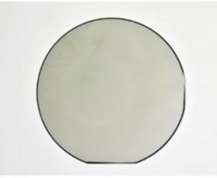
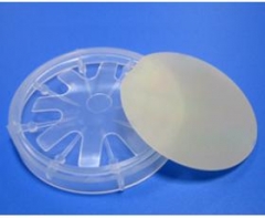
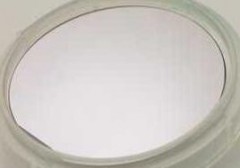
We are manufacturing various types of epi wafer III-V silicon doped n-type semiconductor materials based on Ga, Al, In, As and P grown by MBE or MOCVD. We supply custom structures to meet customer specifications.please contact us for more information.
MOQ :
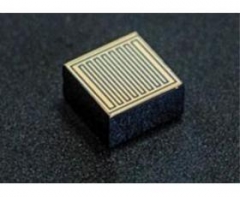
1GaAs Epiwafer
We are manufacturing various types of epi wafer III-V silicon doped n-type semiconductor materials based on Ga, Al, In, As and P grown by MBE or MOCVD. We supply custom structures to meet customer specifications.please contact us for more information.
We have numbers of the United States Veeco's GEN2000, GEN200 large-scale production of epitaxial equipment production line, full set of XRD; PL-Mapping; Surfacescan, and other world-class analysis and testing equipment. The company has more than 12,000 square meters of supporting plant, including world class super-clean semiconductor and a related research and development of the younger generation of clean laboratory facilities
Specification for all new and featured products of MBE III-V compound semiconductor epi wafer:
Substrate Material
Material Capability
Application
GaAs
low temperature GaAs
THz
GaAs
GaAs/GaAlAs/GaAs/GaAs
Schottky Diode
InP
InGaAs
PIN detector
InP
InP/InP/InGaAsP/InP/InGaAs
Laser
GaAs
GaAs/AlAs/GaAs
InP
InP/InAsP/InGaAs/InAsP
GaAs
GaAs/InGaAsN/AlGaAs
/GaAs/AlGaAs
InP
InP/InGaAs/InP
photodetectors
InP
InP/InGaAs/InP
InP
InP/InGaAs
GaAs
GaAs/InGaP/GaAs/AlInP
Solar Cell
/InGaP/AlInP/InGaP/AlInP
GaAs
GaAs/GaInP/GaInAs/GaAs/AlGaAs/GalnP/GalnAs
Solar Cell
/GalnP/GaAs/AlGaAs/AllnP/GalnP/AllnP/GalnAs
InP
InP/GaInP
GaAs
GaAs/AlInP
GaAs
GaAs/AlGaAs/GalnP/AlGaAs/GaAs
703nm Laser
GaAs
GaAs/AlGaAs/GaAs
GaAs
GaAs/AlGaAs/GaAs/AlGaAs/GaAs
HEMT
GaAs
GaAs/AlAs/GaAs/AlAs/GaAs
mHEMT
GaAs
GaAs/DBR/AlGaInP/MQW/AlGaInP/GaP
LED wafer,solid state lighting
GaAs
GaAs/GalnP/AlGaInP/GaInP
635nm,660nm,808nm,780nm, 785nm,
/GaAsP/GaAs/GaAs substrate
950nm, 1300nm,1550nm Laser
GaSb
AlSb/GaInSb/InAs
IR detector,PIN,sensing, IR cemera
silicon
InP or GaAs on Silicon
High speed IC/microprocessors
InSb
Beryllium doped InSb
/ undoped InSb/Te doped InSb/
For more detail specification, please review the following:
LT-GaAs epi layer on GaAs substrate
GaAs Schottky Diode Epitaxial Wafers
InGaAsP/InGaAs on InP substrates
InGaAsN epitaxially on GaAs or InP wafers
Structure for InGaAs photodetectors
AlGaP/GaAs Epi Wafer for Solar Cell
Layer structure of 703nm Laser
GaAs Based Epitaxial Wafer for LED and LD, please see below desc.
Yellow-Green AlGaInP/GaAs LED wafer:565-575nm
GaAs pHEMT epi wafer (GaAs, AlGaAs, InGaAs), please see below desc.
GaAs mHEMT epi wafer (mHEMT: metamorphic high electron mobility transistor)
GaAs HBT epi wafer (GaAs HBT is bipolar junction transistors, which are composed of at least two different semiconductors,which is by GaAs based technology.)Metal-semiconductor field effect transistor (MESFET)
Heterojunction field effect transistor (HFET)
High electron mobility transistor (HEMT)
Pseudomorphic high electron mobility transistor (pHEMT)
Resonant tunnel diode (RTD)
PiN diode
hall effect devices
variable capacitance diode (VCD)
Now we list some specifications:
GaAs HEMT epi wafer, size:2~6inch
|
Item |
Specifications |
Remark |
|
|
Parameter |
Al composition/In composition/Sheet resistance |
Please contact our tech department |
|
|
Hall mobility/2DEG Concentration |
|||
|
Measurement tech |
X-ray diffraction/Eddy current |
Please contact our tech department |
|
|
Un-contact hall |
|||
|
Typical valve |
Struture dependent |
Please contact our tech department |
|
|
5000~6500cm2/V ·S/0.5~1.0x 1012cm-2 |
|||
|
Standard tolerance |
±0.01/±3%/none |
Please contact our tech department |
|
GaAs( gallium arsenide) pHEMT epi wafer,size:2~6inch
|
Item |
Specifications |
Remark |
|
|
Parameter |
Al composition/In composition/Sheet resistance |
Please contact our tech department |
|
|
Hall mobility/2DEG Concentration |
|||
|
Measurement tech |
X-ray diffraction/Eddy current |
Please contact our tech department |
|
|
Un-contact hall |
|||
|
Typical valve |
Struture dependent |
Please contact our tech department |
|
|
5000~6800cm2/V.S/2.0~3.4X1012cm-2 |
|||
|
Standard tolaerance |
±0.01/±3%none |
Please contact our tech department |
|
Remark:GaAs pHEMT: Compared with GaAs HEMT, GaAs PHEMT also incorporates InxGa1-xAs,where InxAs is constrained to x < 0.3 for GaAs-based devices. Structures grown with the same lattice constant as HEMT, but different band gaps are simply referred to as lattice-matched HEMTs.
GaAs mHEMT epi wafer, size:2~6inch
Item
Specifications
Remark
Parameter
In
composition/Sheet resistance
Please contact
our tech department
Hall
mobility/2DEG Concentration
Measurement tech
X-ray
diffraction/Eddy current
Please contact
our tech department
Un-contact hall
Typical valve
Struture
dependent
Please contact
our tech department
8000~10000cm2/V
·S/2.0~3.6x 1012cm-2
Standard
tolerance
±3%/none
Please contact
our tech department
InP HEMT epi wafer,size:2~4inch
|
Item |
Specifications |
Remark |
|
Parameter |
In composition/Sheet resistance/Hall mobility |
Please contact our tech department |
Remark:GaAs(Gallium arsenide) is a compound semiconductor material,a mixture of two elements, gallium (Ga) and arsenic (As). The uses of Gallium arsenide are varied and include being used in LED/LD, field-effect transistors (FETs), and integrated circuits (ICs)
Device applications
RF Switch
Power and low-noise amplifiers
Hall sensor
Optical modulator
Wireless: cell phone or base stations
Automotive radar
MMIC,RFIC
Optical Fiber Communications
GaAs Epi Wafer for LED/IR serie:
1.General description:
1.1 Growth Method: MOCVD
1.2 GaAs epi wafer for Wireless Networking
1.3 GaAs epi wafer for LED /IR and LD/PD
2.Epi wafer specs:
2.1 Wafer size: 2”diameter
2.2Epi Wafer Structure(from top to bottom):
P+GaAs
p-GaP
p-AlGaInP
MQW-AlGaInP
n-AlGaInP
DBR n-ALGaAs/AlAs
Buffer
GaAs substrate
3.Chip sepcification (Base on 9mil*9mil chips)
3.1 Parameter
Chip Size 9mil*9mil
Thickness 190±10um
Electrode diameter 90um±5um
3.2 Optical-elctric characters(Ir=20mA,22℃)
Wavelength 620~625nm
Forward voltage 1.9~2.2v
Reverse voltage ≥10v
Reverse current 0-1uA
3.3 Light intensity characters(Ir=20mA,22℃)
IV(MCD) 80-140
3.4 Epi wafer avelength
Item
Unit
Red
Yellow
Yellow/Green
Description
Wave Length (λD)
nm
585,615,620 ~
630
587 ~ 592
568 ~ 573
IF =20mA
Growth Methods:MOCVD,MBE
epitaxy = growth of film with a crystallographic relationship between film and substrate homoepitaxy (autoepitaxy, isoepitaxy) = film and substrate are same material heteroepitaxy = film and substrate are different materialsPlease more information of growth methods, please click the following:http://www.powerwaywafer.com/Wafer-Technology.html
Remark:
The Chinese government has announced new limits on the exportation of Gallium materials (such as GaAs, GaN, Ga2O3, GaP, InGaAs, and GaSb) and Germanium materials used to make semiconductor chips. Starting from August 1, 2023, exporting these materials is only allowed if we obtains a license from the Chinese Ministry of Commerce. Hope for your understanding and cooperation!
PWAM Develops and manufactures compound semiconductor substrates-gallium arsenide crystal and wafer.We has used advanced crystal growth technology,vertical gradient freeze(VGF) and GaAs wafer processing technology,established a production line from crystal growth, cutting, grinding to polishing processing and built a 100-class clean room for 1
PAM-XIAMEN provides CZT based detectors by solid-state detector technology for x-ray or gamma-ray,which has better energy resolution compared with scintillation crystal based detector, including CZT Planar Detector,CZT Pixilated Detector,CZT Co-Planar Gri
PAM-XIAMEN offers semiconductor silicon carbide wafers,6H SiC and 4H SiC in different quality grades for researcher and industry manufacturers. We has developed SiC crystal growth technology and SiC crystal wafer processing technology,established a production line to manufacturer SiC substrate,Which is applied in GaN epitaxy device,power devices,hi1
PAM-XIAMEN has established the manufacturing technology for freestanding (gallium nitride)GaN substrate wafer, which is for UHB-LED and LD. Grown by hydride vapour phase epitaxy (HVPE) technology,Our GaN substrate has low defect density.
Xiamen Powerway offers GaP wafer - gallium Phosphide which are grown by LEC(Liquid Encapsulated Czochralski) as epi-ready or mechanical grade with n type, p type or semi-insulating in different orientation(111)or(100).
The etching wafer has the characteristics of low roughness, good glossiness and relatively low cost, and directly substitutes the polished wafer or epitaxial wafer which has relatively high cost to produce the electronic elements in some fields, to reduce the costs. There are the low-roughness, low-reflectivity and high-reflectivity etching wafers.
FZ polished wafers, mainly for the production of silicon rectifier (SR), silicon controlled rectifier (SCR), Giant Transistor (GTR), thyristor (GRO)
PAM-XIAMEN Offers Dummy Wafer / Test Wafer / Monitor Wafer
 Contact Information
 luna@powerwaywafer.compowerwaymaterial@gmail.com
  +86-592-5601 404