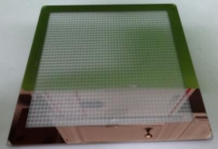
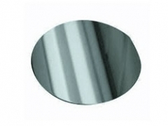
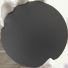
PAM-XIAMEN Offers photoresist plate with photoresist
We can offer Nanolithography (photolithography):Surface preparation, Photoresist apply, Soft bake, Alignment, Exposure, Development,Hard bake, Develop inspect, Etch, Photoresist removal(strip), Final inspection.
MOQ :
1
Nanofabrication
PAM-XIAMEN Offers photoresist plate with photoresist
We can offer Nanolithography (photolithography):Surface preparation, Photoresist apply, Soft bake, Alignment, Exposure, Development,Hard bake, Develop inspect, Etch, Photoresist removal(strip), Final inspection.
A photoresist is a light-sensitive material used in several processes, such as photolithography and photoengraving, to form a patterned coating on a surface, which is crucial in the whole electronic industry.
A positive resist is a type of photoresist in which the portion of the photoresist that is exposed to light becomes soluble to the photoresist developer. The unexposed portion of the photoresist remains insoluble to the photoresist developer.
A negative photoresist is a type of photoresist in which the portion of the photoresist that is exposed to light becomes insoluble to the photoresist developer. The unexposed portion of the photoresist is dissolved by the photoresist developer.
Based on the chemical structure of photoresists, they can be classified into three types:Photopolymeric, photodecomposing, photocrosslinking, photoresist.
Applications:
Microcontact Printing
Fabrication of printed circuit boards (PCB)
Patterning and etching of substrates
Microelectronics
photoresist Microposit
Futurrex
other photoresists,
please contact us for detailed information
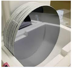
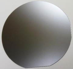
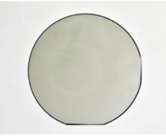
Substrate silicon substrate 2″3″4″5″6″8″
quartz substrate SSP/DSP
glass substrate N/P
SiO2 substrate 100/110/111
other substrate,
please contact us for detailed information
Differences between Positive and Negative Resist
|
Characteristic |
Positive |
Negative |
|
Adhesion to Silicon |
Fair |
Excellent |
|
Relative Cost |
More expensive |
Less expensive |
|
Developer Base |
Aqueous |
Organic |
|
Solubility in the developer |
Exposed region is soluble |
Exposed region is insoluble |
|
Minimum Feature |
0.5 µm |
2 µm |
|
Step Coverage |
Better |
Lower |
|
Wet Chemical Resistance |
Fair |
Excellent |
Basic procedure
A single iteration of photolithography combines several steps in sequence. Modern cleanrooms use automated, robotic wafer track systems to coordinate the process. The procedure described here omits some advanced treatments, such as thinning agents or edge-bead removal.
Cleaning
If organic or inorganic contaminations are present on the wafer surface, they are usually removed by wet chemical treatment, e.g. the RCA clean procedure based on solutions containing hydrogen peroxide. Other solutions made with trichloroethylene, acetone or methanol can also be used to clean.
Preparation
The wafer is initially heated to a temperature sufficient to drive off any moisture that may be present on the wafer surface, 150 °C for ten minutes is sufficient. Wafers that have been in storage must be chemically cleaned to remove contamination. A liquid or gaseous “adhesion promoter”, such as Bis(trimethylsilyl)amine (“hexamethyldisilazane”, HMDS), is applied to promote adhesion of the photoresist to the wafer. The surface layer of silicon dioxide on the wafer reacts with HMDS to form tri-methylated silicon-dioxide, a highly water repellent layer not unlike the layer of wax on a car’s paint. This water repellent layer prevents the aqueous developer from penetrating between the photoresist layer and the wafer’s surface, thus preventing so-called lifting of small photoresist structures in the (developing) pattern. In order to ensure the development of the image, it is best covered and placed over a hot plate and let it dry while stabilizing the temperature at 120 °C.
Photoresist application
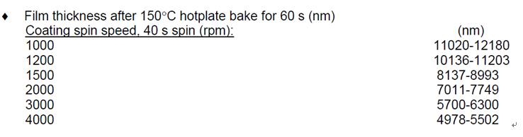
The wafer is covered with photoresist by spin coating. A viscous, liquid solution of photoresist is dispensed onto the wafer, and the wafer is spun rapidly to produce a uniformly thick layer. The spin coating typically runs at 1200 to 4800 rpm for 30 to 60 seconds, and produces a layer between 0.5 and 2.5 micrometres thick. The spin coating process results in a uniform thin layer, usually with uniformity of within 5 to 10 nanometres. This uniformity can be explained by detailed fluid-mechanical modelling, which shows that the resist moves much faster at the top of the layer than at the bottom, where viscous forces bind the resist to the wafer surface. Thus, the top layer of resist is quickly ejected from the wafer’s edge while the bottom layer still creeps slowly radially along the wafer. In this way, any ‘bump’ or ‘ridge’ of resist is removed, leaving a very flat layer. Final thickness is also determined by the evaporation of liquid solvents from the resist. For very small, dense features (< 125 or so nm), lower resist thicknesses (< 0.5 micrometres) are needed to overcome collapse effects at high aspect ratios; typical aspect ratios are < 4:1.
The photo resist-coated wafer is then prebaked to drive off excess photoresist solvent, typically at 90 to 100 °C for 30 to 60 seconds on a hotplate.
Exposure and developing
After prebaking, the photoresist is exposed to a pattern of intense light. The exposure to light causes a chemical change that allows some of the photoresist to be removed by a special solution, called “developer” by analogy with photographic developer. Positive photoresist, the most common type, becomes soluble in the developer when exposed; with negative photoresist, unexposed regions are soluble in the developer.
A post-exposure bake (PEB) is performed before developing, typically to help reduce standing wave phenomena caused by the destructive and constructive interference patterns of the incident light. In deep ultraviolet lithography, chemically amplified resist (CAR) chemistry is used. This process is much more sensitive to PEB time, temperature, and delay, as most of the “exposure” reaction (creating acid, making the polymer soluble in the basic developer) actually occurs in the PEB.
The develop chemistry is delivered on a spinner, much like photoresist. Developers originally often contained sodium hydroxide (NaOH). However, sodium is considered an extremely undesirable contaminant in MOSFET fabrication because it degrades the insulating properties of gate oxides (specifically, sodium ions can migrate in and out of the gate, changing the threshold voltage of the transistor and making it harder or easier to turn the transistor on over time). Metal-ion-free developers such as tetramethylammonium hydroxide (TMAH) are now used.
The resulting wafer is then “hard-baked” if a non-chemically amplified resist was used, typically at 120 to 180 °C[citation needed] for 20 to 30 minutes. The hard bake solidifies the remaining photoresist, to make a more durable protecting layer in future ion implantation, wet chemical etching, or plasma etching.
Etching
In etching, a liquid (“wet”) or plasma (“dry”) chemical agent removes the uppermost layer of the substrate in the areas that are not protected by photoresist. In semiconductor fabrication, dry etching techniques are generally used, as they can be made anisotropic, in order to avoid significant undercutting of the photoresist pattern. This is essential when the width of the features to be defined is similar to or less than the thickness of the material being etched (i.e. when the aspect ratio approaches unity). Wet etch processes are generally isotropic in nature, which is often indispensable for microelectromechanical systems, where suspended structures must be “released” from the underlying layer.
The development of low-defectivity anisotropic dry-etch process has enabled the ever-smaller features defined photolithographically in the resist to be transferred to the substrate material.
Photoresist removal
After a photoresist is no longer needed, it must be removed from the substrate. This usually requires a liquid “resist stripper”, which chemically alters the resist so that it no longer adheres to the substrate. Alternatively, photoresist may be removed by a plasma containing oxygen, which oxidizes it. This process is called ashing, and resembles dry etching. Use of 1-Methyl-2-pyrrolidone (NMP) solvent for photoresist is another method used to remove an image. When the resist has been dissolved, the solvent can be removed by heating to 80 °C without leaving any residue.
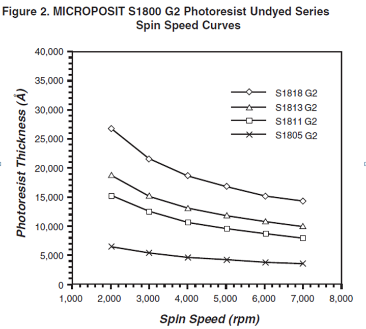
Microposit S1800 G2 Series Photoresist
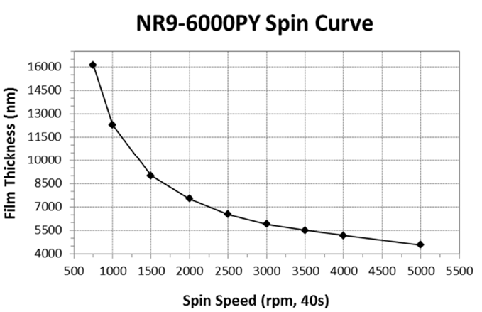
NEGATIVE RESIST NR9-6000PY
NEGATIVE RESIST NR9-6000P
PAM-XIAMEN Offers Photomasks A photo mask is a thin coating of masking material supported by a thicker substrate, and the masking material absorbs light to varying degrees and can be patterned with a custom design. The pattern is used to modulate light and transfer the pattern through the process of photolithography which is the fundamental process1
FZ polished wafers, mainly for the production of silicon rectifier (SR), silicon controlled rectifier (SCR), Giant Transistor (GTR), thyristor (GRO)
Xiamen Powerway offers InAs wafer - Indium arsenide which are grown by LEC(Liquid Encapsulated Czochralski) as epi-ready or mechanical grade with n type, p type or semi-insulating in different orientation(111)or(100).
PAM-XIAMEN offers semiconductor silicon carbide wafers,6H SiC and 4H SiC in different quality grades for researcher and industry manufacturers. We has developed SiC crystal growth technology and SiC crystal wafer processing technology,established a production line to manufacturer SiC substrate,Which is applied in GaN epitaxy device,power devices,hi1
We provide custom thin film (silicon carbide) SiC epitaxy on 6H or 4H substrates for the development of silicon carbide devices. SiC epi wafer is mainly used for Schottky diodes, metal-oxide semiconductor field-effect transistors, junction field effect transistors, bipolar junction transistors, thyristors, GTO, and insulated gate bipolar.
CZ-Silicon The heavily/lightly-doped CZ mono-crystalline silicon is suitable for producing various integrated circuits (IC), diodes, triodes, green-energy solar panel. The special elements (such as Ga, Ge) can be added to produce the high-efficiency, radiation-resistant and anti-degenerating solar cell materials for special components.
Xiamen Powerway offers InSb wafer - Indium antimonide which are grown by LEC(Liquid Encapsulated Czochralski) as epi-ready or mechanical grade with n type, p type or semi-insulating in different orientation(111)or(100).
PAM-XIAMEN is able to offer the following SiC reclaim wafer services.
 Contact Information
 luna@powerwaywafer.compowerwaymaterial@gmail.com
  +86-592-5601 404