Wafer Process:
Wafer Crystal Growth
In the manufacturing of crystal wafers,the first critical step is single crystal growth. Using polycrystal as the raw material with small percent of dopant, such as nitrogen, vanadium,boron or phosphorous. (this dopant determine the electrical properties, or resistivity of the wafers,which is sliced from the crystal), growing ingots through sealed growth furnace.
Wafer Cutting
The seed-end (the top) and the tapered-end (the bottom)of ingots are removed,then the ingot is cut into shorter sections in order to optimize the slicing operation that will follow later. Next,each section is ground to the specified diameter on a mechanical lathe.finally cutting crystal into wafers.
Wafer Polishing
Wafer polishing is required for the wafer fabrication of semiconductor devices.First step is rough lapping by mechanical polishing,second step is thin polishing by CMP(Chemical Mechanical Polishing), to improve the wafer flatness and surface roughness, make its surface to get the precision of epitaxial slice,finally epi-ready wafer becomes.
Wafer Cleaning
During polishing, the wafers are already proceed into a series of cleaning systems.But before the wafers are packaged into containers, they still need to inspect the wafers to see if there are stratches,spots, and inclusions.
Wafer Epitaxy
Epitaxy is a process that grows a thin layer the polished surface of wafer substrate by reactor, and then becomes epiwafer, which provide our customers to build compound semiconductor devices in the world.
Growth and Epitaxy Technology
Hydride Vapour Phase Epitaxy (HVPE) Technology
Grown by HVPE process and technology for the production of compound semiconductors such as GaN, AlN, and AlGaN. They are used in a wide applications:solid state lighting, short wavelength optoelectronics and RF power device.
If you need more information, please view: http://www.powerwaywafer.com/GaN-Templates.html
Molecular Beam Epitaxy(MBE) Technology
MBE is a method of laying down layers of materials with atomic thicknesses on to substrates. This is done by creating a 'molecular beam' of a material which impinges on to the substrate. The resulting 'superlattices' have a number of technologically important uses including Quantum well lasers for semiconducting systems, and Giant Magneto-Resistance for metallic systems.
Metal Organic Chemical Vapor Deposition (MOCVD) Technology
Metal Organic Chemical Vapor Deposition (MOCVD) or Metal-Organic Vapor Phase Epitaxy (MOVPE) is a chemical vapour deposition method for epitaxy by depositing atoms on a wafer substrate.
If you need more information, please view: http://www.powerwaywafer.com/GaAs-Epiwafer.html
And now we give a brief introduction of MBE and MOCVD.
1:MBE
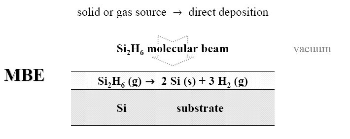
MBE is a method of laying down layers of materials with atomic thicknesses on to substrates. This is done by creating a 'molecular beam' of a material which impinges on to the substrate. The resulting 'superlattices' have a number of technologically important uses including Quantum well lasers for semiconducting systems, and Giant Magneto-Resistance for metallic systems.
In the compound semiconductor industry, using MBE technology,we grow epitaxial layers on GaAs and other compound semiconductor substrates,and offer epi wafers and develop multilayer substrates for for microwaves and RF applications.
1-1:Characteristics of Molecular Beam Epitaxy:
Low growth rate of ~ 1 monolayer (lattice plane) per sec
Low growth temperature (~ 550°C for GaAs)
Smooth growth surface with steps of atomic height and large flat terraces
Precise control of surface composition and morphology
Abrupt variation of chemical composition at interfaces
In-situ control of crystal growth at the atomic level
1-2:Advantages of MBE Technique:
Clean growth environment
Precise control of the beam fluxes
and growth condition
Easy implementation of in situ
diagnostic instruments
Compatibility with other high vacuum
thin-film processing methods (metal
evaporation, ion beam milling, ion implantation)
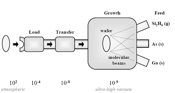
1-3:MBE Process:
2:MOCVD
Metal Organic Chemical Vapor Deposition (MOCVD) or Metal-Organic Vapor Phase Epitaxy (MOVPE) is a chemical vapour deposition method for epitaxy by depositing atoms on a wafer substrate.
The MOCVD principle is quite simple: Atoms that you would like to be in your crystal are combined with complex organic gas molecules and passed over a hot wafer substrate. The heat breaks up the molecules and deposits the desired atoms on the surface, layer by layer. By varying the composition of the gas, we can change the properties of the crystal at an almost atomic scale. It can grow high quality semiconductor layers and the crystal structure of these layers is perfectly aligned with that of the substrate.
 Contact Information
 luna@powerwaywafer.compowerwaymaterial@gmail.com
  +86-592-5601 404


