Due to SiC physical and electronic properties,Silicon Carbide based device are well suitable for short wavelength optoelectronic, high temperature, radiation resistant, and high-power/high-frequency electronic devices,compared with Si and GaAs based device.
SiC Application
Due to SiC physical and electronic properties,Silicon Carbide based device are well suitable for short wavelength optoelectronic, high temperature, radiation resistant, and high-power/high-frequency electronic devices,compared with Si and GaAs based device.
III-V Nitride Deposition
GaN, AlxGa1-xN and InyGa1-yN epitaxial layers on up to SiC substrate or sapphire substrate.
For PAM-XIAMEN Gallium Nitride Epitaxy on Sapphire Templates,please review:
http://www.powerwaywafer.com/GaN-Templates.html
For Gallium Nitride Epitaxy on SiC Templates,which are used to fabrication of blue light emitting diodes and and nearly solar blind UV photodetectors
Optoelectronic Devices
SiC based devices are:
low lattice mismatch forIII-nitride epitaxial layers
high thermal conductivity
monitoring of combustion processes
all sorts of UV-detection
Due to SiC material properties, SiC-based electronics and devices can work in very hostile environment,which can work under high temperature, high power and high radiation conditions
High Power Devices
Due to SiC's properties:
Wide Energy Bandgap (4H-SiC: 3.26eV, 6H-SiC: 3.03eV)
High electrical breakdown field(4H-SiC: 2-4*108 V/m, 6H-SiC: 2-4*108 V/m )
High saturation drift velocity(4H-SiC:2.0*105 m/s, 6H-SiC:2.0*105 m/s)
High thermal conductivity(4H-SiC: 490 W/mK, 6H-SiC: 490 W/mK )
Which are used for fabrication of very high-voltage, high-power devices such as diodes, power transitors, and high power microwave devices.Compared to conventional Si-devices SiC-based power device offers:
faster switching speed
higher voltages
lower parasitic resistances
smaller size
less cooling required due to high-temperature capability
SiC has higher thermal conductivity than GaAs or Si meaning that SiC devices can theoretically operate at higher power densities than either GaAs or Si. Higher thermal conductivity combined with wide bandgap and high critical field give SiC semiconductors an advantage when high power is a key desirable device feature.
Currently silicon carbide (SiC) is widely used for high power MMIC
applications. SiC is also used as a substrate for epitaxial
growth of GaN for even higher power MMIC devices
High Temperature Devices
Due to SiC high thermal conductivity,SiC will conductor heat rapidly than other semiconductor materials.
which enables SiC devices to operate at extremely high power levels and still dissipate the large amounts of excess heat generated
High Frequency Power Devices
SiC-based microwave electronics are used for wireless communications and radar
For detail application of SiC substrate, you can read Detail Application of Silicon Carbide .
We provide custom thin film (silicon carbide) SiC epitaxy on 6H or 4H substrates for the development of silicon carbide devices. SiC epi wafer is mainly used for Schottky diodes, metal-oxide semiconductor field-effect transistors, junction field effect transistors, bipolar junction transistors, thyristors, GTO, and insulated gate bipolar.
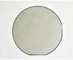
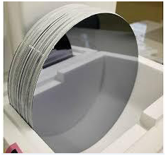
PAM-XIAMEN offers semiconductor silicon carbide wafers,6H SiC and 4H SiC in different quality grades for researcher and industry manufacturers. We has developed SiC crystal growth technology and SiC crystal wafer processing technology,established a production line to manufacturer SiC substrate,Which is applied in GaN epitaxy device,power devices,hi1
PAM-XIAMEN is able to offer the following SiC reclaim wafer services.
FZ polished wafers, mainly for the production of silicon rectifier (SR), silicon controlled rectifier (SCR), Giant Transistor (GTR), thyristor (GRO)
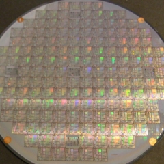
PAM-XIAMEN Offers photoresist plate with photoresist We can offer Nanolithography (photolithography):Surface preparation, Photoresist apply, Soft bake, Alignment, Exposure, Development,Hard bake, Develop inspect, Etch, Photoresist removal(strip), Final inspection.
Gallium Nitride (GaN) HEMTs (High Electron Mobility Transistors) are the next generation of RF power transistor technology.Thanks to GaN technology,PAM-XIAMEN now offer AlGaN/GaN HEMT Epi Wafer on sapphire or Silicon,and AlGaN/GaN on sapphire template.
Xiamen Powerway offers InSb wafer - Indium antimonide which are grown by LEC(Liquid Encapsulated Czochralski) as epi-ready or mechanical grade with n type, p type or semi-insulating in different orientation(111)or(100).
PWAM Develops and manufactures compound semiconductor substrates-gallium arsenide crystal and wafer.We has used advanced crystal growth technology,vertical gradient freeze(VGF) and GaAs wafer processing technology,established a production line from crystal growth, cutting, grinding to polishing processing and built a 100-class clean room for 1
 Contact Information
 luna@powerwaywafer.compowerwaymaterial@gmail.com
  +86-592-5601 404