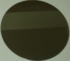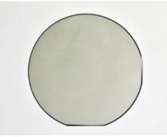
Xiamen Powerway offers InAs wafer - Indium arsenide which are grown by LEC(Liquid Encapsulated Czochralski) as epi-ready or mechanical grade with n type, p type or semi-insulating in different orientation(111)or(100).
Xiamen Powerway offers InAs wafer - Indium arsenide which are grown by LEC(Liquid Encapsulated Czochralski) as epi-ready or mechanical grade with n type, p type or semi-insulating in different orientation(111)or(100).
Indium arsenide, InAs, is a semiconductor composed of indium and arsenic. It has the appearance of grey cubic crystals with a melting point of 942 °C.[2]Indium arsenide is used for construction of infrared detectors, for the wavelength range of 1–3.8 µm. The detectors are usually photovoltaic photodiodes. Cryogenically cooled detectors have lower noise, but InAs detectors can be used in higher-power applications at room temperature as well. Indium arsenide is also used for making of diode lasers.
Indium arsenide is similar to gallium arsenide and is a direct bandgap material. Indium arsenide is sometimes used together with indium phosphide. Alloyed with gallium arsenide it forms indium gallium arsenide - a material with band gap dependent on In/Ga ratio, a method principally similar to alloying indium nitridewith gallium nitride to yield indium gallium nitride.
| Wafer Specification | |
| Item | Specifications |
| Wafer Diameter |
2"50.5±0.5mm 3"76.2±0.4mm |
| Crystal Orientation | (100)±0.1° |
| Thickness |
2"500±25um 3" 625±25um |
| Primary flat length |
2"16±2mm 3"22±2mm |
| Secondary flat length |
2"8±1mm 3"11±1mm |
| Surface Finish | P/E, P/P |
| Package | Epi-Ready,Single wafer container or CF cassette |
| Electrical and Doping Specification | |||||
| Conduction Type | n-type | n-type | n-type | p-type | p-type |
| Dopant | Undoped | Low Sulphur | High Sulphur | Low Zinc | High Zinc |
| E.D.P cm-2 |
2"≤15,000 3"≤50,000 |
||||
| Mobility cm² V-1s-1 | ≥23000 | 25000-15000 | 12000-7000 | 350-200 | 250-100 |
| Carrier Concentration cm-3 | (1-3)*1016 | (4-8)*1016 | (1-3)*1018 | (1-3)*1017 | (1-3)*1018 |
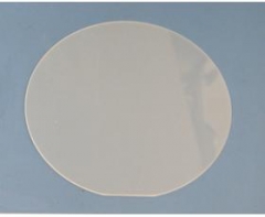
Xiamen Powerway offers InSb wafer - Indium antimonide which are grown by LEC(Liquid Encapsulated Czochralski) as epi-ready or mechanical grade with n type, p type or semi-insulating in different orientation(111)or(100).
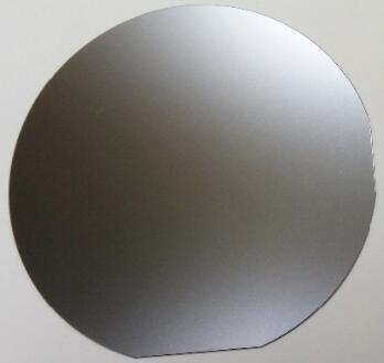
Xiamen Powerway offers InP wafer - Indium Phosphide which are grown by LEC(Liquid Encapsulated Czochralski) or VGF(Vertical Gradient Freeze) as epi-ready or mechanical grade with n type, p type or semi-insulating in different orientation(111)or(100).
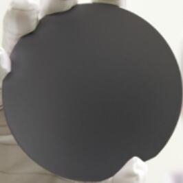
Xiamen Powerway offers GaP wafer - gallium Phosphide which are grown by LEC(Liquid Encapsulated Czochralski) as epi-ready or mechanical grade with n type, p type or semi-insulating in different orientation(111)or(100).
Xiamen Powerway offers GaSb wafer - gallium antimonide which are grown by LEC(Liquid Encapsulated Czochralski) as epi-ready or mechanical grade with n type, p type or semi-insulating in different orientation(111)or(100)
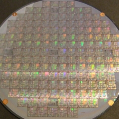
PAM-XIAMEN Offers photoresist plate with photoresist We can offer Nanolithography (photolithography):Surface preparation, Photoresist apply, Soft bake, Alignment, Exposure, Development,Hard bake, Develop inspect, Etch, Photoresist removal(strip), Final inspection.
PAM-XIAMEN offers semiconductor silicon carbide wafers,6H SiC and 4H SiC in different quality grades for researcher and industry manufacturers. We has developed SiC crystal growth technology and SiC crystal wafer processing technology,established a production line to manufacturer SiC substrate,Which is applied in GaN epitaxy device,power devices,hi1
PAM-XIAMEN Offers Dummy Wafer / Test Wafer / Monitor Wafer
We provide custom thin film (silicon carbide) SiC epitaxy on 6H or 4H substrates for the development of silicon carbide devices. SiC epi wafer is mainly used for Schottky diodes, metal-oxide semiconductor field-effect transistors, junction field effect transistors, bipolar junction transistors, thyristors, GTO, and insulated gate bipolar.
 Contact Information
 luna@powerwaywafer.compowerwaymaterial@gmail.com
  +86-592-5601 404