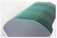
silicon carbide or silicon.PAM-XIAMEN's Template Products enable 20-50% shorter epitaxy cycle times and higher quality epitaxial device layers, with better structural quality and higher thermal conductivity,which can improve devices in the cost, yield, and performance.
MOQ :
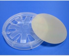
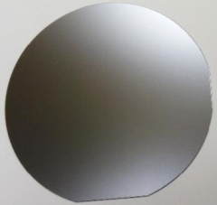
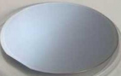
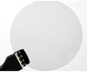
1GaN(gallium nitride ) Templates
PAM-XIAMEN's Template Products consist of crystalline layers of gallium nitride (GaN), aluminum nitride (AlN),aluminum gallium nitride (AlGaN)and indium gallium nitride (InGaN), which are deposited on sapphire substrates. PAM-XIAMEN's Template Products enable 20-50% shorter epitaxy cycle times and higher quality epitaxial device layers, with better structural quality and higher thermal conductivity,which can improve devices in the cost, yield, and performance.
2" GaN Templates Epitaxy on Sapphire Substrates
|
Item |
PAM-2inch-GaNT-N |
PAM-2inch-GaNT-SI |
|
|
Conduction Type |
N-type |
Semi-insulating |
|
|
Dopant |
Si doped or undoped |
Fe doped |
|
|
Size |
2"(50mm) dia. |
||
|
Thickness |
4um,20um,30um,50um,100um |
30um,90um |
|
|
Orientation |
C-axis(0001)+/-1O |
||
|
Resistivity(300K) |
<0.05Ω·cm |
>1x10⁶Ω·cm |
|
|
Dislocation Density |
<1x108cm-2 |
||
|
Substrate Structure |
GaN on Sapphire(0001) |
||
|
Surface Finish |
Single or Double Side Polished,epi-ready |
||
|
Usable Area |
≥ 90 % |
||
2" GaN Templates Epitaxy on Sapphire Substrates
|
Item |
PAM-GaNT-P |
|
Conduction Type |
P-type |
|
Dopant |
Mg doped |
|
Size |
2"(50mm) dia. |
|
Thickness |
5um,20um,30um,50um,100um |
|
Orientation |
C-axis(0001)+/-1O |
|
Resistivity(300K) |
<1Ω·cm or custom |
|
Dopant Concentration |
1E17(cm-3) or custom |
|
Substrate Structure |
GaN on Sapphire(0001) |
|
Surface Finish |
Single or Double Side Polished,epi-ready |
|
Usable Area |
≥ 90 % |
3"GaN Templates Epitaxy on Sapphire Substrates
|
Item |
PAM-3inch-GaNT-N |
|
|
Conduction Type |
N-type |
|
|
Dopant |
Si doped or undoped |
|
|
Exclusion Zone: |
5mm from outer diameter |
|
|
Thickness: |
20um,30um |
|
|
Dislocation density |
< 1x108cm-2 |
|
|
Sheet resistance (300K): |
<0.05Ω·cm |
|
|
Substrate: |
sapphire |
|
|
Orientation : |
C-plane |
|
|
Sapphire thickness: |
430um |
|
|
Polishing: |
Single side Polished,epi-ready, with atomic steps. |
|
|
Backside coating: |
(custom)high quality Titanium coating, thickness > 0.4 μm |
|
|
Packing: |
Individually packed under argon Atmosphere vacuum sealed in class 100 clean room. |
3"GaN Templates Epitaxy on Sapphire Substrates
|
Item |
PAM-3inch-GaNT-SI |
|
|
Conduction Type |
Semi-insulating |
|
|
Dopant |
Fe Doped |
|
|
Exclusion Zone: |
5mm from outer diameter |
|
|
Thickness: |
20um,30um,90um(20um is the best) |
|
|
Dislocation density |
< 1x108cm-2 |
|
|
Sheet resistance (300K): |
>106 ohm.cm |
|
|
Substrate: |
sapphire |
|
|
Orientation : |
C-plane |
|
|
Sapphire thickness: |
430um |
|
|
Polishing: |
Single side Polished,epi-ready, with atomic steps. |
|
|
Backside coating: |
(custom)high quality Titanium coating, thickness > 0.4 μm |
|
|
Packing: |
Individually packed under argon Atmosphere vacuum sealed in class 100 clean room. |
4"GaN Templates Epitaxial on Sapphire Substrates
|
Item |
PAM-4inch-GaNT-N |
|
Conduction Type |
N-type |
|
Dopant |
undoped |
|
Thickness: |
4um |
|
Dislocation density |
< 1x108cm-2 |
|
Sheet resistance (300K): |
<0.05Ω·cm |
|
Substrate: |
sapphire |
|
Orientation : |
C-plane |
|
Sapphire thickness: |
- |
|
Polishing: |
Single side Polished,epi-ready, with atomic steps. |
|
Packing: |
Individually packed under argon Atmosphere vacuum sealed in class 100 clean room. |
2" AlGaN, InGaN, AlN Epitaxy on Sapphire Templates: custom
2”AlN Epitaxy on Sapphire Templates
|
Item |
PAM-AlNT-SI |
|
|
Conduction Type |
semi-insulating |
|
|
Diameter |
Ф 50.8mm ± 1mm |
|
|
Thickness: |
1000nm+/- 10% |
|
|
Substrate: |
sapphire |
|
|
Orientation : |
C-axis(0001)+/-1O |
|
|
Orientation Flat |
A-plane |
|
|
XRD FWHM of (0002) |
<200 arcsec. |
|
|
Useable Surface Area |
≥90% |
|
|
Polishing: |
None |
2”InGaN Epitaxy on Sapphire Templates
|
Item |
PAM-INGAN |
|
|
Conduction Type |
- |
|
|
Diameter |
Ф 50.8mm ± 1mm |
|
|
Thickness: |
100-200nm, custom |
|
|
Substrate: |
sapphire |
|
|
Orientation : |
C-axis(0001)+/-1O |
|
|
Dopant |
In |
|
|
Dislocation Density |
~ 108 cm-2 |
|
|
Useable Surface Area |
≥90% |
|
|
Surface Finish |
Single or Double Side Polished,epi-ready |
2”AlGaN Epitaxy on Sapphire Templates
|
Item |
PAM-AlNT-SI |
|
|
Conduction Type |
semi-insulating |
|
|
Diameter |
Ф 50.8mm ± 1mm |
|
|
Thickness: |
1000nm+/- 10% |
|
|
Substrate: |
sapphire |
|
|
Orientation : |
C-plane |
|
|
Orientation Flat |
A-plane |
|
|
XRD FWHM of (0002) |
<200 arcsec. |
|
|
Useable Surface Area |
≥90% |
|
|
Polishing: |
None |
2"GaN on 4H or 6H SiC substrate
|
1)Undoped GaN buffer or AlN buffer are available; |
||||
|
2)n-type(Si doped or undoped), p-type or semi-insulating GaN epitaxial layers available; |
||||
|
3)vertical conductive structures on n-type SiC; |
||||
|
4)AlGaN – 20-60nm thick, (20%-30%Al), Si doped buffer; |
||||
|
5)GaN n-type layer on 330µm+/-25um thick 2” wafer. |
||||
|
6) Single or double side polished, epi-ready, Ra<0.5um |
||||
|
7)Typical value on XRD: |
||||
|
Wafer ID |
Substrate ID |
XRD(102) |
XRD(002) |
Thickness |
|
#2153 |
X-70105033 (with AlN) |
298 |
167 |
679um |
2" GaN on Silicon Substrate
|
1) GaN layer thickness:50nm-4um; |
|
2) N type or semi-insulating GaN are available; |
|
3) Single or double side polished, epi-ready, Ra<0.5um |
Hydride Vapour Phase Epitaxy (HVPE) process
Grown by HVPE process and technology for the production of compound semiconductors such as GaN, AlN, and AlGaN. They are used in a wide applications:solid state lighting, short wavelength optoelectronics and RF power device.
In the HVPE process, Group III nitrides (such as GaN, AlN) are formed by reacting hot gaseous metal chlorides (such as GaCl or AlCl) with ammonia gas (NH3). The metal chlorides are generated by passing hot HCl gas over the hot Group III metals. All reactions are done in a temperature controlled quartz furnace.
Remark:
The Chinese government has announced new limits on the exportation of Gallium materials (such as GaAs, GaN, Ga2O3, GaP, InGaAs, and GaSb) and Germanium materials used to make semiconductor chips. Starting from August 1, 2023, exporting these materials is only allowed if we obtains a license from the Chinese Ministry of Commerce. Hope for your understanding and cooperation!
PAM-XIAMEN has established the manufacturing technology for freestanding (gallium nitride)GaN substrate wafer, which is for UHB-LED and LD. Grown by hydride vapour phase epitaxy (HVPE) technology,Our GaN substrate has low defect density.
PAM-XIAMEN's GaN(gallium nitride)-based LED epitaxial wafer is for ultra high brightness blue and green light emitting diodes (LED) and laser diodes (LD) application.
Gallium Nitride (GaN) HEMTs (High Electron Mobility Transistors) are the next generation of RF power transistor technology.Thanks to GaN technology,PAM-XIAMEN now offer AlGaN/GaN HEMT Epi Wafer on sapphire or Silicon,and AlGaN/GaN on sapphire template.
FZ-Silicon The mono-crystalline silicon with the characteristics of low foreign-material content, low defect density and perfect crystal structure is produced with the float-zone process; no foreign material is introduced during the crystal growth. The FZ-Silicon conductivity is usually above 1000 Ω-cm, and the FZ-Silicon is mainly used to produce 1
FZ polished wafers, mainly for the production of silicon rectifier (SR), silicon controlled rectifier (SCR), Giant Transistor (GTR), thyristor (GRO)
Xiamen Powerway offers InAs wafer - Indium arsenide which are grown by LEC(Liquid Encapsulated Czochralski) as epi-ready or mechanical grade with n type, p type or semi-insulating in different orientation(111)or(100).
Silicon Epitaxial Wafer(Epi Wafer) is a layer of single crystal silicon deposited onto a single crystal silicon wafer(note: it is available to Grow a layer of poly crystalline Silicon layer on top of a highly doped Singly crystalline Silicon wafer,but it needs buffer layer (such as oxide or poly-Si) in between the bulk Si substrate and the top epit1
Xiamen Powerway offers GaSb wafer - gallium antimonide which are grown by LEC(Liquid Encapsulated Czochralski) as epi-ready or mechanical grade with n type, p type or semi-insulating in different orientation(111)or(100)
 Contact Information
 luna@powerwaywafer.compowerwaymaterial@gmail.com
  +86-592-5601 404