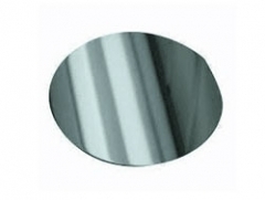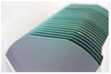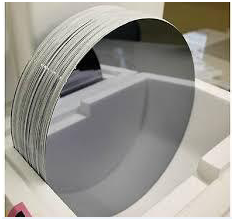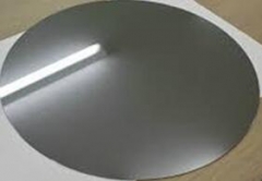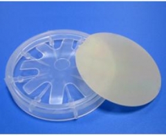
PAM-XIAMEN Offers Dummy Wafer / Test Wafer / Monitor Wafer
Test Wafer Monitor Wafer Dummy Wafer
PAM-XIAMEN Offers Dummy Wafer / Test Wafer / Monitor Wafer
Dummy wafers (also called as test wafers) are wafers mainly used for experiment and test and being different
from general wafers for product. Accordingly, reclaimed wafers are mostly applied as dummy wafers (test wafers).
Dummy wafers are often used in a production device to improve safety in the beginning of production process and
are used for delivery check and evaluation of process form. As dummy wafers are often used for experiment and test,
size and thickness thereof are important factors in most occasions.
In each process, film thickness, pressure resistance, reflection index and presence of pinball are measured using
dummy wafers (test wafers). Also, dummy wafers (test wafers) are used for measurement of pattern size, check
of defect and so on in lithography.
Monitor wafers are the wafers to be used in the case that an adjustment is required in each production step
prior to the actual IC production. For example, when the conditions of each process are set, such as the case of
measuring tolerance of device against ( the variation of ) substrate thickness, monitor wafers are being used as
a substitution of high-standard and high value wafers. Moreover, they are also used for the monitoring purpose in
the process together with product wafers. Monitor wafers are necessary wafer materials as important as product
prime wafers. They are also called as test wafers together with dummy wafers.
For more product detail or if you have required specification, please contact us at luna@powerwaywafer.com or powerwaymaterial@gmail.com.
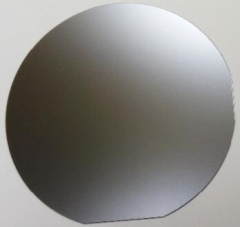
Test Wafer
Single Side Polished Test Wafer N Type (200Nos)
|
Sl No |
Item |
SCL SPECIFICATIONS |
|
|
1 |
Growing method |
CZ |
|
|
2 |
Wafer Diameter |
150 ± 0.5mm |
|
|
3 |
Wafer Thickness |
675±25 µm |
|
|
4 |
Wafer Surface Orientation |
<100>±2° |
|
|
5 |
Dopant |
Phosphorus |
|
|
6 |
Dislocation Density |
Less than 5000/cm2 |
|
|
8 |
Resistivity |
4-7Ωcm |
|
|
9 |
Radial Resistivity Variation (max.) |
15% |
|
|
10 |
Flatness |
|
|
|
10a |
· BOW (max.) |
60 µm |
|
|
10b |
· TIR (max.) |
6 µm |
|
|
10c |
· TAPER (max.) |
12 µm |
|
|
10d |
· WARP (max.) |
60 µm |
|
|
11 |
Primary Flat |
|
|
|
11a |
· Length |
57.5±2.5 mm |
|
|
11b |
· Orientation |
{110}±2° as per SEMI Standard |
|
|
11c |
Secondary Flat |
As per SEMI Standard |
|
|
12 |
Front Surface Finish |
Mirror Polished |
|
|
13 |
Max. particles of size ≥0.3µm |
30 |
|
|
14 |
· Scratches, Haze, Edge Chips, Orange Peel & Other defects |
Nil |
|
|
15 |
Back Surface |
Damage free Etched |
|
|
16 |
Packing Requirement |
Should be vacuum sealed in Class ’10’environment in double layer packing.Wafers should be shipped in Fluorware ORION TWO wafer shippers or equivalent make made from ultra clean polypropylene |
|
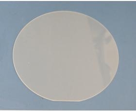
Double Side Polished Test Wafer N Type (150 Nos)
|
Sl No |
Item |
SCL SPECIFICATIONS |
|
|
1 |
Growing method |
CZ |
|
|
2 |
Wafer Diameter |
150 ± 0.5mm |
|
|
3 |
Wafer Thickness |
675±25µm |
|
|
4 |
Wafer Surface Orientation |
<100>±2° |
|
|
5 |
Dopant |
Phosphorus |
|
|
6 |
Dislocation Density |
Less than 5000/cm2 |
|
|
8 |
Resistivity |
4-7Ωcm |
|
|
9 |
Radial Resistivity Variation (max.) |
15% |
|
|
10 |
Flatness |
|
|
|
10a |
· BOW (max.) |
60 µm |
|
|
10b |
· TIR (max.) |
6 µm |
|
|
10c |
· TAPER (max.) |
12 µm |
|
|
10d |
· WARP (max.) |
60 µm |
|
|
11 |
Primary Flat |
|
|
|
11a |
· Length |
57.5±2.5 mm |
|
|
11b |
· Orientation |
{110}±2° as per SEMI Standard |
|
|
11c |
Secondary Flat |
As per SEMI Standard |
|
|
12 |
Front Surface Finish |
Mirror Polished |
|
|
13 |
Max. particles of size ≥0.3µm |
30 |
|
|
14 |
· Scratches, Haze, Edge Chips, |
Nil |
|
|
Orange Peel & Other defects |
|||
|
15 |
Back Surface |
Mirror Polished |
|
|
16 |
Packing Requirement |
Should be vacuum
sealed in Class ’10’ |
|
Monitor Wafer / Dummy Wafer
Monitor / Dummy Silicon wafer
|
Wafer Diameter |
Polished |
Wafer Surface |
Wafer Thickness |
Resistivity |
Particle |
|
Orientation |
|||||
|
4″ |
1 side |
100/111 |
250-500μm |
0-100 |
0.2μm≤qty30 |
|
6″ |
1 side |
100 |
500-675μm |
0-100 |
0.2μm≤qty30 |
|
8″ |
1 side |
100 |
600-750μm |
0-100 |
0.2μm≤qty30 |
|
12″ |
2 side |
100 |
650-775μm |
0-100 |
0.09μm≤qty100 |
REGENERATED 200mm WAFERS
|
Item# |
PARAMETER |
Units |
Value |
Notes |
|
|
1 |
Growth Method |
|
CZ |
|
|
|
2 |
Orientation |
|
1-0-0 |
|
|
|
3 |
Resistivity |
Ωм.см |
1-50 |
|
|
|
4 |
Type / dopant |
|
р,n/ |
|
|
|
Boron, Phosphorus |
|||||
|
5 |
Thickness |
мкм |
1гр. – 620, |
|
|
|
2гр. – 650 |
|||||
|
3гр. – 680 |
|||||
|
4гр. – 700 |
|||||
|
5гр. – 720 |
|||||
|
6 |
GBIR (TTV |
мкм |
1-3гр. <30, |
|
|
|
4-5гр. <20 |
|||||
|
7 |
GLFR (TIR |
мкм |
<10 |
|
|
|
8 |
Warp |
мкм |
<60 |
|
|
|
9 |
Bow |
мкм |
<40 |
|
|
|
10 |
Metal contamination |
1/см2 |
<3E10 |
|
|
|
11 |
Front surface |
|
Polished |
|
|
|
12 |
Front surface visual: |
|
|
|
|
|
Haze, Scratches, Stains, Spots |
|
none |
|||
|
Orange Peel |
|
none |
|||
|
Cracks, Craters |
|
none |
|||
|
13 |
Front Side LPD: |
|
|
Number of wafers with stated parameter value should be not less than 80% of batch, |
|
|
< 0,12мкм |
|
<100 |
|||
|
<0,16мкм |
|
<50 |
|||
|
<0,20мкм |
|
<20 |
|||
|
<0,30мкм |
|
<10 |
|
FZ-Silicon The mono-crystalline silicon with the characteristics of low foreign-material content, low defect density and perfect crystal structure is produced with the float-zone process; no foreign material is introduced during the crystal growth. The FZ-Silicon conductivity is usually above 1000 Ω-cm, and the FZ-Silicon is mainly used to produce 1
CZ-Silicon The heavily/lightly-doped CZ mono-crystalline silicon is suitable for producing various integrated circuits (IC), diodes, triodes, green-energy solar panel. The special elements (such as Ga, Ge) can be added to produce the high-efficiency, radiation-resistant and anti-degenerating solar cell materials for special components.
Silicon Epitaxial Wafer(Epi Wafer) is a layer of single crystal silicon deposited onto a single crystal silicon wafer(note: it is available to Grow a layer of poly crystalline Silicon layer on top of a highly doped Singly crystalline Silicon wafer,but it needs buffer layer (such as oxide or poly-Si) in between the bulk Si substrate and the top epit1
FZ polished wafers, mainly for the production of silicon rectifier (SR), silicon controlled rectifier (SCR), Giant Transistor (GTR), thyristor (GRO)
The etching wafer has the characteristics of low roughness, good glossiness and relatively low cost, and directly substitutes the polished wafer or epitaxial wafer which has relatively high cost to produce the electronic elements in some fields, to reduce the costs. There are the low-roughness, low-reflectivity and high-reflectivity etching wafers.
We provide custom thin film (silicon carbide) SiC epitaxy on 6H or 4H substrates for the development of silicon carbide devices. SiC epi wafer is mainly used for Schottky diodes, metal-oxide semiconductor field-effect transistors, junction field effect transistors, bipolar junction transistors, thyristors, GTO, and insulated gate bipolar.
PAM-XIAMEN has established the manufacturing technology for freestanding (gallium nitride)GaN substrate wafer, which is for UHB-LED and LD. Grown by hydride vapour phase epitaxy (HVPE) technology,Our GaN substrate has low defect density.
Xiamen Powerway offers InAs wafer - Indium arsenide which are grown by LEC(Liquid Encapsulated Czochralski) as epi-ready or mechanical grade with n type, p type or semi-insulating in different orientation(111)or(100).
 Contact Information
 luna@powerwaywafer.compowerwaymaterial@gmail.com
  +86-592-5601 404