Gallium Nitride (GaN) HEMTs (High Electron Mobility Transistors) are the next generation of RF power transistor technology.Thanks to GaN technology,PAM-XIAMEN now offer AlGaN/GaN HEMT Epi Wafer on sapphire or Silicon,and AlGaN/GaN on sapphire template.
MOQ :
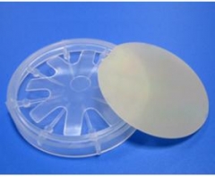
12" GaN HEMT Epitaxial Wafers
We offer 2" GaN HEMT Wafers, the structure is as follows:
Structure(from top to bottom):
*undoped GaN cap(2~3nm)
AlxGa1-xN (18~40nm)
AlN(buffer layer)
un-doped GaN(2~3um)
Sapphire substrate
* We can use Si3N to replace GaN on the top, the adhesion is strong, it is coated by sputter or PECVD.
AlGaN/GaN HEMT Epi Wafer on sapphire/GaN
|
Layer ID |
Layer Name |
Material |
Al Content(%) |
Dopant |
Thickness(nm) |
|
0 |
Substrate |
GaN or Sapphire |
﹍ |
﹍ |
﹍ |
|
1 |
Nucleation Layer |
Various,AlN |
100 |
DID |
﹍ |
|
2 |
Buffer Layer |
GaN |
0 |
NID |
1800 |
|
3 |
Spacer |
AlN |
100 |
NID |
1 |
|
4 |
Schottky Barrier |
AlGaN |
20 or 23 or 26 |
NID |
21 |
2",4" AlGaN/GaN HEMT Epi Wafer on Si
1.1Specifications for Aluminium Gallium Nitride (AlGaN) / Gallium Nitride (GaN) High Electron Mobility Transistor (HEMT) on Silicon substrate.
|
Requirements |
Specification |
|
AlGaN/GaN HEMT Epi Wafer on Si |
|
|
AlGaN/GaN HEMT structure |
Refer 1.2 |
|
Substrate Material |
Silicon |
|
Orientation |
<111> |
|
Growth method |
Float Zone |
|
Conduction Type |
P or N |
|
Size (inch) |
2”,4” |
|
Thickness(μm) |
625 |
|
Backside |
Rough |
|
Resistivity(Ω-cm) |
>6000 |
|
Bow(μm) |
≤ ±35 |
1.2.Epistructure: Crack-free Epilayers
Layer #
Composition
Thickness
X
Dopant
Carrier Concentration
5
GaN
2nm
-
-
-
4
AlxGa1–xN
8nm
0.26
-
-
3
AlN
1nm
Un-doped
2
GaN
≥1000 nm
Un-doped
1
Buffer/Transition
Layer
-
-
Substrate
Silicon
350µm/625µm
-
1.3.Electrical Properties of the AlGaN/GaN HEMT structure
2DEG Mobility (at 300 K) :≥1,800 cm2/V.s
2DEG Sheet Carrier Density (at 300 K) :≥0.9x1013 cm-2
RMS Roughness (AFM) : ≤ 0.5 nm (5.0 µm × 5.0 µm scan Area)
2"AlGaN/GaN on sapphire
For specification of AlGaN/GaN on sapphire template, please contact our sales department: sales@powerwaywafer.com.
Application: Used in blue laser diodes, ultraviolet LEDs (down to 250 nm), and AlGaN/GaN HEMTs device.
Explanation of AlGaN/Al/GaN HEMTs:
Nitride HEMTs are being intensively developed for high-power electronics in high-frequency amplification and power switching applications. Often high performance in DC operation is lost when the HEMT is switched – for example, the on-current collapses when the gate signal is pulsed. It is thought that such effects are related to charge trapping that masks the effect of the gate on current flow. Field-plates on the source and gate electrodes have been used to manipulate the electric field in the device, mitigating such current-collapse phenomena.
GaN EpitaxialTechnology—-Customized GaN epitaxy on SiC,Si and Sapphire substrate for HEMTs, LEDs:
Related Classification:
algan/gan hemt, algan/gan hemt band diagram, algan/gan hemt based biosensor, algan gan hemt phd thesis, algan/gan hemt based liquid sensors, algan/gan hemt reliability, algan/gan hemt with 300-ghz, algan gan hemts an overview of device, algan gan hemt characterization, algan/gan hemts with an ingan-based back-barrier, aln/gan hemt, algan/aln/gan hemt, inaln/aln/gan hemt, aln passivation gan hemt.
Remark:
The Chinese government has announced new limits on the exportation of Gallium materials (such as GaAs, GaN, Ga2O3, GaP, InGaAs, and GaSb) and Germanium materials used to make semiconductor chips. Starting from August 1, 2023, exporting these materials is only allowed if we obtains a license from the Chinese Ministry of Commerce. Hope for your understanding and cooperation!
PAM-XIAMEN's Template Products consist of crystalline layers of gallium nitride (GaN), aluminum nitride (AlN),aluminum gallium nitride (AlGaN)and indium gallium nitride (InGaN), which are deposited on sapphire substrates, silicon carbide or silicon.PAM-XIAMEN's Template Products enable 20-50% shorter epitaxy cycle times and higher quality epitaxial1
PAM-XIAMEN has established the manufacturing technology for freestanding (gallium nitride)GaN substrate wafer, which is for UHB-LED and LD. Grown by hydride vapour phase epitaxy (HVPE) technology,Our GaN substrate has low defect density.
PAM-XIAMEN's GaN(gallium nitride)-based LED epitaxial wafer is for ultra high brightness blue and green light emitting diodes (LED) and laser diodes (LD) application.
PAM-XIAMEN Offers Dummy Wafer / Test Wafer / Monitor Wafer
PAM-XIAMEN's GaN(gallium nitride)-based LED epitaxial wafer is for ultra high brightness blue and green light emitting diodes (LED) and laser diodes (LD) application.
FZ-Silicon The mono-crystalline silicon with the characteristics of low foreign-material content, low defect density and perfect crystal structure is produced with the float-zone process; no foreign material is introduced during the crystal growth. The FZ-Silicon conductivity is usually above 1000 Ω-cm, and the FZ-Silicon is mainly used to produce 1
Cadmium Zinc Telluride (CdZnTe or CZT) is a new semiconductor, which enables to convert radiation to electron effectively, it is mainly used in infrared thin-film epitaxy substrate,X-ray detectors and Gamma-ray detectors, laser optical modulation, high-performance solar cells and other high-tech fields.
We are manufacturing various types of epi wafer III-V silicon doped n-type semiconductor materials based on Ga, Al, In, As and P grown by MBE or MOCVD. We supply custom structures to meet customer specifications.please contact us for more information.
 Contact Information
 luna@powerwaywafer.compowerwaymaterial@gmail.com
  +86-592-5601 404