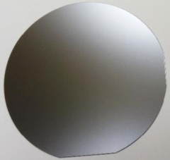
Cadmium Zinc Telluride (CdZnTe or CZT) is a new semiconductor, which enables to convert radiation to electron effectively, it is mainly used in infrared thin-film epitaxy substrate,X-ray detectors and Gamma-ray detectors, laser optical modulation, high-performance solar cells and other high-tech fields.
CdZnTe (CZT) Wafer
Cadmium Zinc Telluride (CdZnTe or CZT) is a new semiconductor, which enables to convert radiation to electron effectively, it is mainly used in infrared thin-film epitaxy substrate,X-ray detectors and Gamma-ray detectors, laser optical modulation, high-performance solar cells and other high-tech fields.
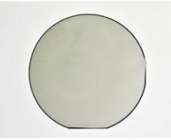
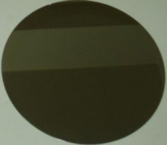
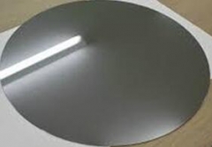
From 2001,PAM-XIAMEN offers commercial CZT wafers with high quality and very competitive price. We also can offer CZT crystals with contacts. Regulaly contacts of anodes and cathode are both deposited by Au, but we can use Al to the deposit the contacts as required.And we offer wafer custom size.
Market of Nuclear Radication:
Traditional Nuclear Radiation Spectrometers: Ge – High energy resolution, but cryogenic cooling required; NaI Scintillators – Low energy resolution Room-Temperature Wide Band-gap Semiconductor Spectrometers: No cooling requirements: High energy resolution; High spatial resolution
CdZnTe growth:
There are three growth method: Bridgman, THM, and floating zone.CZT Grown crystals are difficuilt in comparison to Ge and Si(Czochralski), the reason is:
• Te-reach secondary phases (inclusions and precipitates)
• Twinning
• Subgrain boundaries
CdZnTe Material Application:
Nuclear Radiation is mainly application:X-ray diffraction,X-ray fluorescence, bone densitometry, CT scanners,flat panel, Cardiology,Molecular breast imaging, surgical probes, and all other activities using nuclear radiations. Generally speaking, CZT material is used in the following field:
1.National and Homeland Security
• Nonproliferation of nuclear materials
• Secondary inspection for portals
• Safeguards measurements: custom inspection systems, radiation monitoring for nuclear safeguard
• Forensics and attribution
• Nuclear waste management
2.Medical Imaging
• SPECT, PET and CT scanners
• Bone densitometers
• Medical probes
3.Basic science
• Astrophysics
• Gamma-Ray Spectroscopy
• Synchrotron X-ray research
4.Industrial imaging
• Bore-hole logging
• X-ray and gamma-ray cameras
• XRF material analyses
5.PV thin film solar panel:
CdZnTe Material Products and Service:
It is mainly used in infrared thin-film epitaxy substrate and radiation detection:
1.CdZnTe For epitaxial growth, HgCdTe:
CZT substrate
size
20x20 +/-0.1mm
or larger
CZT structure
undoped
twin-free
CZT thickness
1000 +/- 50
Zinc
Distribution
4.5% or custom
"y" %
wafer to wafer
<4% +/- 1%
"y" %
within wafer
<4% +/- 0.5%
Orientation
(211)B,(111)B
DCRC FWHM
<= 50 arc.sec
Carrier
concentration
-
IR transmission
% (2-20)um
>60%
Precipitate size
<5um
Precipitate
density
<1E4 cm-2
Etch pit
density
<=1E5 cm-2
Surface, B-face
EPI ready
Surface, A-face
Roughly polished
Surface
roughness
Ra<20A or
custom
Te precipitate
size
<5um
Face
identification
A face
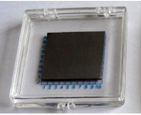
2.CdZnTe for radiation detection:
PAM-XIAMEN offer CdZnTe material:
As cut wafer; wafer size could be custom, for regular wafer size, please see wafer list
Polished wafer; wafer size could be custom
With contacts/ electrodes available;
With PCB board available;
With pixel available;
With BNC available
And now we list some detail application and explanations for your reference:
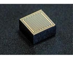
2.1.CdZnTe for nuclear radiation detection (X, gamma,beta, thermal, neutron,counter & spectrometer):
It is an important national security need to be able to ubiquitously deploy high resolution (preferably room temperature)
gamma detectors in the field to provide unambiguous identification of special nuclear materials (SNM) as well as other potential threats.
The energy resolution for semiconductor-based gamma detectors is defined as the full width at half maximum (FWHM) of a peak divided by the energy of the peak. The ideal characteristic would be an impulse function. This, however, is not the case in practice and the detected signals can be challenging to resolve and interpret.
And we can offer CZT material with the following features to meet this application:
1)Cd(1-x)Zn(x)Te
2)High resolution FWHM@59.5 keV<?(please contact with our sales team)
3)Good mu-tao value
2.2.For CZT sensors:
2.3.CdZnTe For CZT gamma cameras:
The CZT based camera features high spatial resolution, high-energy resolution, a reduced dead space on the edge of the field of view, and a compact format. The camera performance was first examined by comparison of small field of view examinations with those from an Elscint SP6HR standard clinical gamma camera. The new camera was found to give equal or improved image quality. The camera was then used for a systematic phantom study of small lesions in a background as would be found in breast cancer imaging. In this study the camera was able to systematically detect smaller, deeper, and fainter lesions. The camera is presently being used in a clinical trial aimed to assess its value in scintimammography where previous limitations of image quality and detector size have restricted the use of the functional imaging techniques. Preliminary results show high sensitivity and specificity with respect to X-ray mammography and surgery.
And we can offer CZT material with the following features to meet this application:
1)High resolution:
2)Low to mid energy isotopes (50keV to 180keV) available, as well as high energy isotopes;
3)With/without guard ring
2.4.CdZnTe for solar cell:
N type or p type are available.
2.5.CdZnTe for gamma spectroscopy and gamma-ray:
And we can offer CZT material with the following features to meet this application:
1)Both pixelated and coplanar available
2)with Ohmic and Schottky contact available
2.6.CdZnTe for electro-optic application -light modulation
For detailed quotes and special requirements please contact our sales office.
PAM-XIAMEN provides CZT based detectors by solid-state detector technology for x-ray or gamma-ray,which has better energy resolution compared with scintillation crystal based detector, including CZT Planar Detector,CZT Pixilated Detector,CZT Co-Planar Gri
PAM-XIAMEN offers semiconductor silicon carbide wafers,6H SiC and 4H SiC in different quality grades for researcher and industry manufacturers. We has developed SiC crystal growth technology and SiC crystal wafer processing technology,established a production line to manufacturer SiC substrate,Which is applied in GaN epitaxy device,power devices,hi1
Xiamen Powerway offers InP wafer - Indium Phosphide which are grown by LEC(Liquid Encapsulated Czochralski) or VGF(Vertical Gradient Freeze) as epi-ready or mechanical grade with n type, p type or semi-insulating in different orientation(111)or(100).
The etching wafer has the characteristics of low roughness, good glossiness and relatively low cost, and directly substitutes the polished wafer or epitaxial wafer which has relatively high cost to produce the electronic elements in some fields, to reduce the costs. There are the low-roughness, low-reflectivity and high-reflectivity etching wafers.
We provide custom thin film (silicon carbide) SiC epitaxy on 6H or 4H substrates for the development of silicon carbide devices. SiC epi wafer is mainly used for Schottky diodes, metal-oxide semiconductor field-effect transistors, junction field effect transistors, bipolar junction transistors, thyristors, GTO, and insulated gate bipolar.
Xiamen Powerway offers InAs wafer - Indium arsenide which are grown by LEC(Liquid Encapsulated Czochralski) as epi-ready or mechanical grade with n type, p type or semi-insulating in different orientation(111)or(100).
PWAM Develops and manufactures compound semiconductor substrates-gallium arsenide crystal and wafer.We has used advanced crystal growth technology,vertical gradient freeze(VGF) and GaAs wafer processing technology,established a production line from crystal growth, cutting, grinding to polishing processing and built a 100-class clean room for 1
Gallium Nitride (GaN) HEMTs (High Electron Mobility Transistors) are the next generation of RF power transistor technology.Thanks to GaN technology,PAM-XIAMEN now offer AlGaN/GaN HEMT Epi Wafer on sapphire or Silicon,and AlGaN/GaN on sapphire template.
 Contact Information
 luna@powerwaywafer.compowerwaymaterial@gmail.com
  +86-592-5601 404