MOQ :
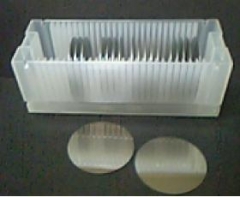
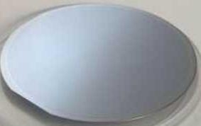
1Xiamen Powerway offers GaP wafer - gallium Phosphide which are grown by LEC(Liquid Encapsulated Czochralski) as epi-ready or mechanical grade with n type, p type or semi-insulating in different orientation(111)or(100).
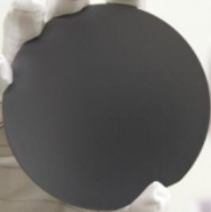
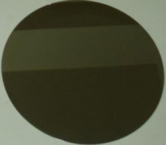
Gallium phosphide (GaP), a phosphide of gallium, is a compound semiconductor material with an indirect band gap of 2.26eV(300K). The polycrystalline material has the appearance of pale orange pieces. Undoped single crystal wafers appear clear orange, but strongly doped wafers appear darker due to free-carrier absorption. It is odorless and insoluble in water.Sulfur or tellurium are used as dopants to produce n-type semiconductors. Zinc is used as a dopant for the p-type semiconductor.Gallium phosphide has applications in optical systems. Its refractive index is between 4.30 at 262 nm (UV), 3.45 at 550 nm (green) and 3.19 at 840 nm (IR).
| Specs of GaP Wafer and Substrate | |
| Conducion Type | N-type |
| Dopant | S doped |
| Wafer Diameter | 50.8+/-0.5mm |
| Crystal Orientation | (111)+/-0.5° |
| Flat orientation | 111 |
| Flat length | 17.5+/-2mm |
| Carrier Concentration | (2-7)x10^7/cm3 |
| Resistivity at RT | 0.05-0.4ohm.cm |
| Mobility | >100cm²/V.sec |
| Etch Pit Density | <3*10^5/cm² |
| Laser Marking | upon request |
| Suface Fnish | P/E |
| Thickness | 250+/-20um |
| Epi Ready | Yes |
| Package | Single wafer container or cassette |
Remark:
The Chinese government has announced new limits on the exportation of Gallium materials (such as GaAs, GaN, Ga2O3, GaP, InGaAs, and GaSb) and Germanium materials used to make semiconductor chips. Starting from August 1, 2023, exporting these materials is only allowed if we obtains a license from the Chinese Ministry of Commerce. Hope for your understanding and cooperation!
Xiamen Powerway offers InSb wafer - Indium antimonide which are grown by LEC(Liquid Encapsulated Czochralski) as epi-ready or mechanical grade with n type, p type or semi-insulating in different orientation(111)or(100).
Xiamen Powerway offers InP wafer - Indium Phosphide which are grown by LEC(Liquid Encapsulated Czochralski) or VGF(Vertical Gradient Freeze) as epi-ready or mechanical grade with n type, p type or semi-insulating in different orientation(111)or(100).
Xiamen Powerway offers InAs wafer - Indium arsenide which are grown by LEC(Liquid Encapsulated Czochralski) as epi-ready or mechanical grade with n type, p type or semi-insulating in different orientation(111)or(100).
Xiamen Powerway offers GaSb wafer - gallium antimonide which are grown by LEC(Liquid Encapsulated Czochralski) as epi-ready or mechanical grade with n type, p type or semi-insulating in different orientation(111)or(100)
Silicon Epitaxial Wafer(Epi Wafer) is a layer of single crystal silicon deposited onto a single crystal silicon wafer(note: it is available to Grow a layer of poly crystalline Silicon layer on top of a highly doped Singly crystalline Silicon wafer,but it needs buffer layer (such as oxide or poly-Si) in between the bulk Si substrate and the top epit1
PAM offers semiconductor materials,single crystal (Ge)Germanium Wafer grown by VGF / LEC
Gallium Nitride (GaN) HEMTs (High Electron Mobility Transistors) are the next generation of RF power transistor technology.Thanks to GaN technology,PAM-XIAMEN now offer AlGaN/GaN HEMT Epi Wafer on sapphire or Silicon,and AlGaN/GaN on sapphire template.
PAM-XIAMEN's GaN(gallium nitride)-based LED epitaxial wafer is for ultra high brightness blue and green light emitting diodes (LED) and laser diodes (LD) application.
 Contact Information
 luna@powerwaywafer.compowerwaymaterial@gmail.com
  +86-592-5601 404