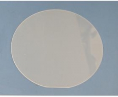
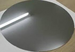
FZ-Silicon
The mono-crystalline silicon with the characteristics of low foreign-material content, low defect density and perfect crystal structure is produced with the float-zone process; no foreign material is introduced during the crystal growth. The FZ-Silicon conductivity is usually above 1000 Ω-cm, and the FZ-Silicon is mainly used to produce the high inverse-voltage elements and photoelectronic devices.
Float-zone mono-crystalline silicon
FZ-Silicon
The mono-crystalline silicon with the characteristics of low foreign-material content, low defect density and perfect crystal structure is produced with the float-zone process; no foreign material is introduced during the crystal growth. The FZ-Silicon conductivity is usually above 1000 Ω-cm, and the FZ-Silicon is mainly used to produce the high inverse-voltage elements and photoelectronic devices.
NTDFZ-Silicon
The mono-crystalline silicon with high-resistivity and uniformity can be achieved by neutron irradiation of FZ-silicon, to ensure the yield and uniformity of produced elements, and is mainly used to produce the silicon rectifier (SR), silicon control (SCR), giant transistor (GTR), gate-turn-off thyristor (GTO), static induction thyristor (SITH), insulate-gate bipolar transistor (IGBT), extra HV diode (PIN), smart power and power IC, etc; it is the main functional material for various frequency converters, rectifiers, large-power control elements, new power electronic devices, detectors, sensors, photoelectronic devices and special power devices..
GDFZ-Silicon
Utilizing the foreign-material diffusion mechanism, add the gas-phase foreign-material during the float-zone process of monocrystalline silicon, to solve the doping problem of float-zone process from the root, and to get the GDFZ-silicon which is N-type or P-type, has the resistivity 0.001-300 Ω.cm, relative good resistivity uniformity and neutron irradiation. It is applicable for producing various semi-conductor power elements, insulate-gate bipolar transistor (IGBT) and high-efficiency solar cell, etc.
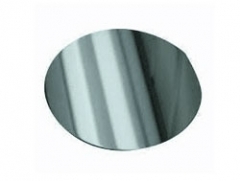
CFZ-Silicon
The monocrystalline-silicon is produced with the combination of Czochralski and float-zone processes, and has the quality between the CZ monocrystalline silicon and FZ monocrystalline silicon; the special elements can be doped, such as the Ga, Ge and others. The new-generation CFZ silicon solar wafers are better than various silicon wafers in global PV industry on each performance index; the conversion efficiency of solar panel is up to 24-26%. The products are mainly applied in the high-efficiency solar batteries with the special structure, back-contact, HIT and other special processes, and more widely used in the LED, power elements, automobile, satellite and other various products and fields.
Our advantages at a glance
1.Advanced epitaxy growth equipment and test equipment.
2.Offer the highest quality with low defect density and good surface roughness.
3.Strong research team support and technology support for our customers
Type
Conduction Type
Orientation
Diameter(mm)
Conductivity(Ω•cm)
High resistance
N&P
<100>&<111>
76.2-200
>1000
NTD
N
<100>&<111>
76.2-200
30-800
CFZ
N&P
<100>&<111>
76.2-200
1-50
GD
N&P
<100>&<111>
76.2-200
0.001-300
Wafer specification
|
Ingot Parameter |
Item |
Description |
|
Growing method |
FZ |
|
|
Orientation |
<111> |
|
|
Off-orientation |
4±0.5 degree to the nearest <110> |
|
|
Type/Dopant |
P/Boron |
|
|
Resistivity |
10-20 W.cm |
|
|
RRV |
≤15% (Max edge-Cen)/Cen |
|
Wafer Parameter |
Item |
Description |
|
Diameter |
150±0.5 mm |
|
|
Thickness |
675±15 um |
|
|
Primary Flat Length |
57.5±2.5 mm |
|
|
Primary Flat Orientation |
<011>±1 degree |
|
|
Secondary Flat Length |
None |
|
|
Secondary Flat Orientation |
None |
|
|
TTV |
≤5 um |
|
|
Bow |
≤40 um |
|
|
Warp |
≤40 um |
|
|
Edge Profile |
SEMI Standard |
|
|
Front Surface |
Chemical-Mechenical Polishing |
|
|
LPD |
≥0.3 um@≤15 pcs |
|
|
Back Surface |
Acid Etched |
|
|
Edge Chips |
None |
|
|
Package |
Vacuum Packing; Inner Plastic, Outer Aluminum |
PAM-XIAMEN Offers Dummy Wafer / Test Wafer / Monitor Wafer
CZ-Silicon The heavily/lightly-doped CZ mono-crystalline silicon is suitable for producing various integrated circuits (IC), diodes, triodes, green-energy solar panel. The special elements (such as Ga, Ge) can be added to produce the high-efficiency, radiation-resistant and anti-degenerating solar cell materials for special components.
Silicon Epitaxial Wafer(Epi Wafer) is a layer of single crystal silicon deposited onto a single crystal silicon wafer(note: it is available to Grow a layer of poly crystalline Silicon layer on top of a highly doped Singly crystalline Silicon wafer,but it needs buffer layer (such as oxide or poly-Si) in between the bulk Si substrate and the top epit1
FZ polished wafers, mainly for the production of silicon rectifier (SR), silicon controlled rectifier (SCR), Giant Transistor (GTR), thyristor (GRO)
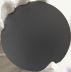
The etching wafer has the characteristics of low roughness, good glossiness and relatively low cost, and directly substitutes the polished wafer or epitaxial wafer which has relatively high cost to produce the electronic elements in some fields, to reduce the costs. There are the low-roughness, low-reflectivity and high-reflectivity etching wafers.
Xiamen Powerway offers InSb wafer - Indium antimonide which are grown by LEC(Liquid Encapsulated Czochralski) as epi-ready or mechanical grade with n type, p type or semi-insulating in different orientation(111)or(100).
Gallium Nitride (GaN) HEMTs (High Electron Mobility Transistors) are the next generation of RF power transistor technology.Thanks to GaN technology,PAM-XIAMEN now offer AlGaN/GaN HEMT Epi Wafer on sapphire or Silicon,and AlGaN/GaN on sapphire template.
Due to SiC physical and electronic properties,Silicon Carbide based device are well suitable for short wavelength optoelectronic, high temperature, radiation resistant, and high-power/high-frequency electronic devices,compared with Si and GaAs based device.
 Contact Information
 luna@powerwaywafer.compowerwaymaterial@gmail.com
  +86-592-5601 404