MOQ :
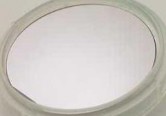
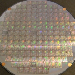
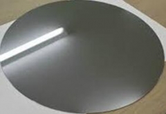
1Freestanding GaN substrate
PAM-XIAMEN has established the manufacturing technology for freestanding (Gallium Nitride)GaN substrate wafer which is for UHB-LED and LD. Grown by hydride vapour phase epitaxy (HVPE) technology,Our GaN substrate has low defect density and less or free macro defect density.
Specification of Freestanding GaN substrate
Here shows detail specification:
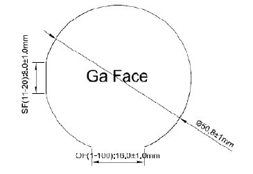
2"Free-standing (gallium nitride) GaN Substrate
|
Item |
PAM-FS-GaN50-N |
PAM-FS-GaN50-SI |
|
|
Conduction Type |
N-type |
Semi-insulating |
|
|
Size |
2"(50.8)+/-1mm |
||
|
Thickness |
300+/-50um |
||
|
Orientation |
C-axis(0001)+/-0.5o |
||
|
Primary Flat Location |
(1-100)+/-0.5o |
||
|
Primary Flat Length |
16+/-1mm |
||
|
Secondary Flat Location |
(11-20)+/-3o |
||
|
Secondary Flat Length |
8+/-1mm |
||
|
Resistivity(300K) |
<0.5Ω·cm |
>106Ω·cm |
|
|
Dislocation Density |
<5x106cm-2 |
||
|
Marco Defect Density |
A grade<=2cm-2 B grade>2cm-2 |
||
|
TTV |
<=15um |
||
|
BOW |
<=20um |
||
|
Surface Finish |
Front Surface:Ra<0.2nm.Epi-ready polished |
||
Back Surface:1.Fine ground 2.Rough grinded
Usable Area≥ 90 %
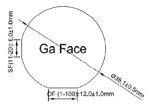
1.5"Free-standing GaN Substrate
|
Item |
PAM-FS-GaN38-N |
PAM-FS-GaN38-SI |
|
|
Conduction Type |
N-type |
Semi-insulating |
|
|
Size |
1.5"(38.1)+/-0.5mm |
||
|
Thickness |
260+/-20um |
||
|
Orientation |
C-axis(0001)+/-0.5o |
||
|
Primary Flat Location |
(1-100)+/-0.5o |
||
|
Primary Flat Length |
12+/-1mm |
||
|
Secondary Flat Location |
(11-20)+/-3o |
||
|
Secondary Flat Length |
6+/-1mm |
||
|
Resistivity(300K) |
<0.5Ω·cm |
>106Ω·cm |
|
|
Dislocation Density |
<5x106cm-2 |
||
|
Marco Defect Density |
A grade<=2cm-2 B grade>2cm-2 |
||
|
TTV |
<=15um |
||
|
BOW |
<=20um |
||
|
Surface Finish |
Front Surface:Ra<0.2nm.Epi-ready polished |
||
Back Surface:1.Fine ground 2.Rough grinded
Usable Area≥ 90 %
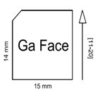
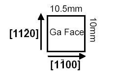
15mm,10mm,5mm Free-standing GaN Substrate
|
Item |
PAM-FS-GaN15-N PAM-FS-GaN10-N PAM-FS-GaN5-N |
PAM-FS-GaN15-SI PAM-FS-GaN10-SI PAM-FS-GaN5-SI |
|
|
Conduction Type |
N-type |
Semi-insulating |
|
|
Size |
14.0mm*15mm 10.0mm*10.5mm 5.0*5.5mm |
||
|
Thickness |
230+/-20um, 280+/-20um |
||
|
Orientation |
C-axis(0001)+/-0.5o |
||
|
Primary Flat Location |
|
||
|
Primary Flat Length |
|
||
|
Secondary Flat Location |
|
||
|
Secondary Flat Length |
|
||
|
Resistivity(300K) |
<0.5Ω·cm |
>106Ω·cm |
|
|
Dislocation Density |
<5x106cm-2 |
||
|
Marco Defect Density |
0cm-2 |
||
|
TTV |
<=15um |
||
|
BOW |
<=20um |
||
|
Surface Finish |
Front Surface:Ra<0.2nm.Epi-ready polished |
||
Back Surface:1.Fine ground 2.Rough grinded
Usable Area≥ 90 %
Note:
Validation Wafer:Considering convenience of usage, PAM-XIAMEN offer 2" Sapphire Validation wafer for below 2" size Freestanding GaN Substrate
Application of GaN Substrate
Solid State Lighting:GaN devices are used as ultra high brightness light emitting diodes (LEDs), TVs, automobiles, and general lighting
DVD Storage: Blue laser diodes
Power Device: GaN devices are used as various components in high-power and high-frequency power electronics like cellular base stations, satellites, power amplifiers, and inverters/converters for electric vehicles (EV) and hybrid electric vehicles (HEV). GaN's low sensitivity to ionizing radiation (like other group III nitrides) makes it a suitable material for spaceborne applications such as solar cell arrays for satellites and high-power, high-frequency devices for communication, weather, and surveillance satellites
Ideal for III-Nitrides re-growth
Wireless Base Stations: RF power transistors
Wireless Broadband Access: high frequency MMICs,RF-Circuits MMICs
Pressure Sensors:MEMS
Heat Sensors: Pyro-electric detectors
Power Conditioning: Mixed signal GaN/Si Integration
Automotive Electronics: High temperature electronics
Power Transmission Lines: High voltage electronics
Frame Sensors: UV detectors
Solar Cells:GaN's wide band gap covers the solar spectrum from 0.65 eV to 3.4 eV (which is practically the entire solar spectrum), making indium gallium nitride
(InGaN) alloys perfect for creating solar cell material. Because of this advantage, InGaN solar cells grown on GaN substrates are poised to become one of the most important new applications and growth market for GaN substrate wafers.
Ideal for HEMTs, FETs
GaN Schottky diode project: We accept custom spec of Schottky diodes fabricated on the HVPE-grown, free-standing gallium nitride (GaN) layers of n- and p-types.
Both contacts (ohmic and Schottky) were deposited on the top surface using Al/Ti and Pd/Ti/Au.
Remark:
The Chinese government has announced new limits on the exportation of Gallium materials (such as GaAs, GaN, Ga2O3, GaP, InGaAs, and GaSb) and Germanium materials used to make semiconductor chips. Starting from August 1, 2023, exporting these materials is only allowed if we obtains a license from the Chinese Ministry of Commerce. Hope for your understanding and cooperation!
PAM-XIAMEN's Template Products consist of crystalline layers of gallium nitride (GaN), aluminum nitride (AlN),aluminum gallium nitride (AlGaN)and indium gallium nitride (InGaN), which are deposited on sapphire substrates, silicon carbide or silicon.PAM-XIAMEN's Template Products enable 20-50% shorter epitaxy cycle times and higher quality epitaxial1
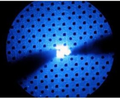
PAM-XIAMEN's GaN(gallium nitride)-based LED epitaxial wafer is for ultra high brightness blue and green light emitting diodes (LED) and laser diodes (LD) application.
Gallium Nitride (GaN) HEMTs (High Electron Mobility Transistors) are the next generation of RF power transistor technology.Thanks to GaN technology,PAM-XIAMEN now offer AlGaN/GaN HEMT Epi Wafer on sapphire or Silicon,and AlGaN/GaN on sapphire template.
PAM-XIAMEN is able to offer the following SiC reclaim wafer services.
Xiamen Powerway offers GaP wafer - gallium Phosphide which are grown by LEC(Liquid Encapsulated Czochralski) as epi-ready or mechanical grade with n type, p type or semi-insulating in different orientation(111)or(100).
PAM-XIAMEN Offers photoresist plate with photoresist We can offer Nanolithography (photolithography):Surface preparation, Photoresist apply, Soft bake, Alignment, Exposure, Development,Hard bake, Develop inspect, Etch, Photoresist removal(strip), Final inspection.
The etching wafer has the characteristics of low roughness, good glossiness and relatively low cost, and directly substitutes the polished wafer or epitaxial wafer which has relatively high cost to produce the electronic elements in some fields, to reduce the costs. There are the low-roughness, low-reflectivity and high-reflectivity etching wafers.
PAM-XIAMEN's GaN(gallium nitride)-based LED epitaxial wafer is for ultra high brightness blue and green light emitting diodes (LED) and laser diodes (LD) application.
 Contact Information
 luna@powerwaywafer.compowerwaymaterial@gmail.com
  +86-592-5601 404