Who We Are

As the lead manufacturer of compound semiconductor material in China. PAM-XIAMEN develops advanced crystal growth and epitaxy technologies, range from the first generation Germanium wafer, second generation Gallium Arsenide with substrate growth and epitaxy on III-V silicon doped n-type semiconducto1
Read More

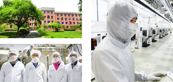
After more than 20 years of accumulation and development, our company has an obvious advantage in technology innovation and talent pool. 

In the future,We need to speed up the pace of actual action to provide customers with better products and services

Doctor Chan -CEO Of Xiamen Powerway Advanced Material Co., Ltd

Our Products

blue laser

GaN Templates

PAM-XIAMEN's Template Products consist of crystalline layers of gallium nitride (GaN), aluminum nitride (AlN),aluminum gallium nitride (AlGaN)and indium gallium nitride (InGaN), which are deposited on sapphire substrates, silicon carbide or silicon.PAM-XIAMEN's Template Products enable 20-50% shorter epitaxy cycle times and higher quality epitaxial1

gan on silicon

Freestanding GaN substrate

PAM-XIAMEN has established the manufacturing technology for freestanding (gallium nitride)GaN substrate wafer, which is for UHB-LED and LD. Grown by hydride vapour phase epitaxy (HVPE) technology,Our GaN substrate has low defect density.

GaAs crystal

GaAs (Gallium Arsenide) Wafers

PWAM Develops and manufactures compound semiconductor substrates-gallium arsenide crystal and wafer.We has used advanced crystal growth technology,vertical gradient freeze(VGF) and GaAs wafer processing technology,established a production line from crystal growth, cutting, grinding to  polishing processing and built a 100-class clean room for 1

sic crystal

SiC Epitaxy

We provide custom thin film (silicon carbide) SiC epitaxy on 6H or 4H substrates for the development of silicon carbide devices. SiC epi wafer is mainly used for Schottky diodes, metal-oxide semiconductor field-effect transistors, junction field effect transistors, bipolar junction transistors, thyristors, GTO, and insulated gate bipolar.

sic crystal

SiC Substrate

PAM-XIAMEN offers semiconductor silicon carbide wafers,6H SiC and 4H SiC in different quality grades for researcher and industry manufacturers. We has developed SiC crystal growth technology and SiC crystal wafer processing technology,established a production line to manufacturer SiC substrate,Which is applied in GaN epitaxy device,power devices,hi1

gan expitaxy

GaN based LED Epitaxial Wafer

PAM-XIAMEN's GaN(gallium nitride)-based LED epitaxial wafer is for ultra high brightness blue and green light emitting diodes (LED) and laser diodes (LD) application.

gan HEMT epitaxy

GaN HEMT epitaxial wafer

Gallium Nitride (GaN) HEMTs (High Electron Mobility Transistors) are the next generation of RF power transistor technology.Thanks to GaN technology,PAM-XIAMEN now offer AlGaN/GaN HEMT Epi Wafer on sapphire or Silicon,and AlGaN/GaN on sapphire template.

sic crystal

SiC Wafer Reclaim

PAM-XIAMEN is able to offer the following SiC reclaim wafer services.

Why Choose Us

  • Free And Professional Technology Support

    You can get our free technology service from enquiry to after service based on our 25+ experiences in semiconductor line.

  • Good Sales Service

    Our goal is to meet all of your requirements, no matter how small orders and how difficult questions they may be, to maintain sustained and profitable growth for every customer through our qualified products and satisfying service.

  • 25+ Years Experiences

    With more than 25+years experiences in compound semiconductor material field and export business, our team can assure you that we can understand your requirements and deal with your project professionally.

  • Reliable Quality

    Quality is our first priority. PAM-XIAMEN has been ISO9001:2008, owns and shares four modern facories which can provide quite a big range of qualified products to meet different needs of our customers, and every order has to be handled through our rigorous quality system. Test report is provided for1

"We have been using the Powerway epi wafers for some of our work.We are very impressed with the quality of the epi"
James S.Speck, Materials Department University of California
2018-01-25
"Dear PAM-XIAMEN teams, thank you for your profession opinion, the problem was solved, we are so glad to be your partner"
Raman K. Chauhan, Seren Photonics
2018-01-25
"Thank you for quick reply of my questions and competitive price, it is very useful for us, we will order again soon"
Markus Sieger, University of Ulm
2018-01-25
"The silicon carbide wafers have arrived today,and we really pleased with them! Thumbs up to your production crew!"
Dennis, University of Exeter
2018-01-25

The World’s Most Famous Universities & Companies Trust Us

Latest News

Density Functional Theory Calculations of Atomic Configurations and Bandgaps of C-, Ge-, and Sn-Doped Si Crystals for Solar Cells

2020-03-17

Poly-Si crystals are mainly used in solar cells because of their low cost. Here, the zones of sensitivity to wavelengths in sunlight should be expanded to increase the engineering efficiency of solar cells. Group IV compound semiconductors films, e.g., Si (Ge) films doped with C, Ge (C, Si), and/or Sn atoms with contents of several %, on a Si or Ge substrate have been identified as potential solutions to this technical problem. In this study, we calculated the formation energy of each atomic configuration of C, Ge, and Sn atoms in Si by using density functional theory. The "Hakoniwa" method proposed by Kamiyama et al. [Materials Science in Semiconductor Processing, 43, 209 (2016)] was applied to a 64-atom supercell of Si including up to three atoms of C, Ge, and/or Sn (up to 4.56%) in order to obtain the ratio of each atomic configuration and the average value of the Si bandgaps. Not only the conventional generalized gradient approximation (GGA) but also the screened-exchange local-den...

Read More

Electrical Conductivity of Direct Wafer-Bonded GaAs/GaAs Structures for Wafer-Bonded Tandem Solar Cells

2020-03-09

Source:IOPscience For more information, please visit our website: www.semiconductorwafers.net, send us email at sales@powerwaywafer.com or powerwaymaterial@gmail.com

Read More

Optical Transmission, Photoluminescence, and Raman Scattering of Porous SiC Prepared from p-Type 6H SiC

2020-03-05

The optical transmission, temperature-dependence of the photoluminescence (PL), and Raman scattering of porous SiC prepared from p-type 6H-SiC are compared with those from bulk p-type 6H-SiC. While the transmission spectrum of bulk SiC at room temperature reveals a relatively sharp edge corresponding to its band gap at 3.03 eV, the transmission edge of porous SiC (PSC) is too wide to determine its band gap. It is believed that this wide edge might be due to surface states in PSC. At room temperature, the PL from PSC is 20 times stronger than that from bulk SiC. The PL PSC spectrum is essentially independent of temperature. The relative intensities of the Raman scattering peaks from PSC are largely independent of the polarization configuration, in contrast to those from bulk SiC, which suggests that the local order is fairly random. Source:IOPscience For more information, please visit our website: www.semiconductorwafers.net, send us email at sales@powerwaywafer.com&...

Read More

Upgrading of CdZnTe by annealing with pure Cd and Zn metals

2020-02-25

1−y alloy as the annealing source.

Read More

Fabrication of InP/SiO2/Si Substrate using Ion-Cutting Process and Selective Chemical Etching

2020-02-18

In this study, an InP layer was transferred onto a Si substrate coated with a thermal oxide, through a process combining ion-cutting process and selective chemical etching. Compared with conventional ion-cutting of bulk InP wafers, this layer transfer scheme not only takes advantage of ion- cutting by saving the remaining substrates for reuse, but also takes advantage of selective etching to improve the transferred surface conditions without using the chemical and mechanical polishing. An InP/InGaAs/InP heterostructure initially grown by MOCVD was implanted with H+ ions. The implanted heterostructure was bonded to a Si wafer coated with a thermal SiO2 layer. Upon subsequent annealing, the bonded structure exfoliated at the depth around the hydrogen projected range located in the InP substrate. Atomic force microscopy showed that after selective chemical etchings on the as-transferred structure, a final structure of InP/SiO2/Si was obtained with a relatively smooth surface. Source:IOPsc...

Read More

A review on MBE-grown HgCdSe infrared materials on GaSb (211)B substrates

2020-02-12

We review our recent efforts on developing HgCdSe infrared materials on GaSb substrates via molecular beam epitaxy (MBE) for fabricating next generation infrared detectors with features of lower production cost and larger focal plane array format size. In order to achieve high-quality HgCdSe epilayers, ZnTe buffer layers are grown before growing HgCdSe, and the study of misfit strain in ZnTe buffer layers shows that the thickness of ZnTe buffer layer needs to be below 300 nm in order to minimize the generation of misfit dislocations. The cut-off wavelength/alloy composition of HgCdSe materials can be varied in a wide range by varying the ratio of Se/Cd beam equivalent pressure during the HgCdSe growth. Growth temperature presents significant impact on the material quality of HgCdSe, and lower growth temperature leads to higher material quality for HgCdSe. Typically, long-wave infrared HgCdSe (x=0.18, cut-off wavelength of  at 80 K) presents an electron mobility as high as&nbs...

Read More

The Electrochemical Society Wet Etching Technology for Semiconductor and Solar Silicon Manufacturing: Part 2 - Process, Equipment and Implementation

2020-01-20

Wet etching is an important step in the manufacturing of semiconductor and solar wafers and for the production of MEMS devices. While it has been replaced by the more precise dry etching technology in advanced semiconductor device fabrication, it still plays an important role in the manufacture of the silicon substrate itself. It is also used for providing stress relief and surface texturing of solar wafers in high volume. The technology of wet etching silicon for semiconductor and solar applications will be reviewed. Impact on this step for wafer properties and critical parameters (flatness, topology and surface roughness for semiconductor wafers, surface texture and reflectance for solar wafers) will be presented. The rationale for the use of a etching technology and etchant for specific applications in semiconductor and solar wafer manufacturing will be presented. Source:IOPscience For more information, please visit our website: www.semiconductorwafers.net, send us email at&nbs...

Read More

Characterization of 4H-SiC Homoepitaxial Films on Porous 4H-SiC from Bis(trimethylsilyl)methane Precursor

2020-01-13

4H-SiC homoepitaxial films were grown on 8° off-axis porous 4H-SiC (0001) faces in the temperature range of  by chemical vapor deposition from bis(trimethylsilyl)methane (BTMSM) precursor. The activation energy for growth was 5.6 kcal/mol, indicating that the film growth is dominated by the diffusion-limited mechanism. Triangular stacking faults were incorporated in the SiC thin film grown at low temperature of 1280°C due to the formation of 3C-SiC polytype. Moreover, super-screw dislocations appeared seriously in the SiC film grown below 1320°C. Clean and featureless morphology was observed in the SiC film grown below 25 standard cubic centimeters per minute (sccm)  carrier gas flow rate of BTMSM at 1380°C while 3C-SiC polytype with double positioning boundaries grew at 30 sccm flow rate of BTMSM. The dislocation density of the epi layer was strongly influenced by the growth temperature and flow rate of BTMSM. Double axis crystal X-ray diffraction and optical micro...

Read More

Density Functional Theory Study of the Stress Impact on Formation Enthalpy of Intrinsic Point Defect around Dopant Atom in Ge Crystal

2020-01-07

During the last decade, the use of single crystal germanium (Ge) layers and structures in combination with silicon (Si) substrates has led to a revival of defect research on Ge. In Si crystals, dopants and stresses affect the intrinsic point defect (vacancy V and self-interstitial I) parameters and thus change the thermal equilibrium concentrations of V and I Source:IOPscience For more information, please visit our website: www.semiconductorwafers.net, send us email at sales@powerwaywafer.com or powerwaymaterial@gmail.com

Read More

Contact Us

If you would like a quotation or more information about our products, please leave us a message, will reply you as soon as possible.
   
Contact Us Contact Us 
If you would like a quotation or more information about our products, please leave us a message, will reply you as soon as possible.