PAM-XIAMEN offers semiconductor silicon carbide wafers,6H SiC and 4H SiC in different quality grades for researcher and industry manufacturers. We has developed SiC crystal growth technology and SiC crystal wafer processing technology,established a production line to manufacturer SiC substrate,Which is applied in GaN epitaxy device,power devices,high-temperature device and optoelectronic Devices. As a professional company invested by the leading manufacturers from the fields of advanced and high-tech material research and state institutes and China's Semiconductor Lab,we are devoted to continuously improve the quality of currently substrates and develop large size substrates.
MOQ :
1
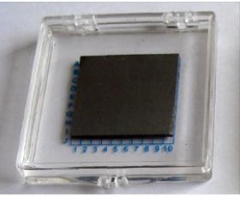
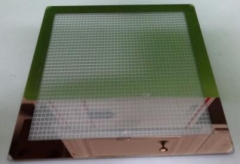
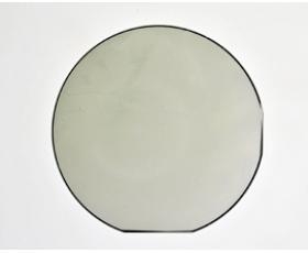
Silicon Carbide Wafers
PAM-XIAMEN offers semiconductor silicon carbide wafers,6H SiC and 4H SiC in different quality grades for researcher and industry manufacturers. We has developed SiC crystal growth technology and SiC crystal wafer processing technology,established a production line to manufacturer SiC substrate,Which is applied in GaN epitaxy device,power devices,high-temperature device and optoelectronic Devices. As a professional company invested by the leading manufacturers from the fields of advanced and high-tech material research and state institutes and China's Semiconductor Lab,we are devoted to continuously improve the quality of currently substrates and develop large size substrates.
Here shows detail specification:
SILICON CARBIDE MATERIAL PROPERTIES
|
Polytype |
Single Crystal 4H |
Single Crystal 6H |
|
Lattice Parameters |
a=3.076 Å |
a=3.073 Å |
|
|
c=10.053 Å |
c=15.117 Å |
|
Stacking Sequence |
ABCB |
ABCACB |
|
Band-gap |
3.26 eV |
3.03 eV |
|
Density |
3.21 · 103 kg/m3 |
3.21 · 103 kg/m3 |
|
Therm. Expansion Coefficient |
4-5×10⁻⁶/K |
4-5×10⁻⁶/K |
|
Refraction Index |
no = 2.719 |
no = 2.707 |
|
|
ne = 2.777 |
ne = 2.755 |
|
Dielectric Constant |
9.6 |
9.66 |
|
Thermal Conductivity |
490 W/mK |
490 W/mK |
|
Break-Down Electrical Field |
2-4 · 108 V/m |
2-4 · 108 V/m |
|
Saturation Drift Velocity |
2.0 · 105 m/s |
2.0 · 105 m/s |
|
Electron Mobility |
800 cm2/V·S |
400 cm2/V·S |
|
hole Mobility |
115 cm2/V·S |
90 cm2/V·S |
|
Mohs Hardness |
~9 |
~9 |
6H N-TYPE SIC, 2″WAFER SPECIFICATION
|
SUBSTRATE PROPERTY |
S6H-51-N-PWAM-250 S6H-51-N-PWAM-330 S6H-51-N-PWAM-430 |
|
Description |
A/B Production Grade C/D Research Grade D Dummy Grade 6H SiC Substrate |
|
Polytype |
6H |
|
Diameter |
(50.8 ± 0.38) mm |
|
Thickness |
(250 ± 25) μm (330 ± 25) μm (430 ± 25) μm |
|
Carrier Type |
n-type |
|
Dopant |
Nitrogen |
|
Resistivity (RT) |
0.02 ~ 0.1 Ω·cm |
|
Surface Roughness |
< 0.5 nm (Si-face CMP Epi-ready); <1 nm (C- face Optical polish) |
|
FWHM |
A<30 arcsec B/C/D <50 arcsec |
|
Micropipe Density |
A+≤1cm-2 A≤10cm-2 B≤30cm-2 C≤50cm-2 D≤100cm-2 |
|
Surface Orientation |
|
|
On axis |
<0001>± 0.5° |
|
Off axis |
3.5° toward <11-20>± 0.5° |
|
Primary flat orientation |
Parallel {1-100} ± 5° |
|
Primary flat length |
16.00 ± 1.70 mm |
|
Secondary flat orientation |
Si-face:90° cw. from orientation flat ± 5° |
|
C-face:90° ccw. from orientation flat ± 5° |
|
|
Secondary flat length |
8.00 ± 1.70 mm |
|
Surface Finish |
Single or double face polished |
|
Packaging |
Single wafer box or multi wafer box |
|
Usable area |
≥ 90 % |
|
Edge exclusion |
1 mm |
4H SEMI-INSULATING SIC, 2″WAFER SPECIFICATION
(High-Purity Semi-Insulating(HPSI) SiC substrate is available)
|
SUBSTRATE PROPERTY |
S4H-51-SI-PWAM-250 S4H-51-SI-PWAM-330 S4H-51-SI-PWAM-430 |
|
Description |
A/B Production Grade C/D Research Grade D Dummy Grade 4H SEMI Substrate |
|
Polytype |
4H |
|
Diameter |
(50.8 ± 0.38) mm |
|
Thickness |
(250 ± 25) μm (330 ± 25) μm (430 ± 25) μm |
|
Resistivity (RT) |
>1E5 Ω·cm |
|
Surface Roughness |
< 0.5 nm (Si-face CMP Epi-ready); <1 nm (C- face Optical polish) |
|
FWHM |
A<30 arcsec B/C/D <50 arcsec |
|
Micropipe Density |
A+≤1cm-2 A≤10cm-2 B≤30cm-2 C≤50cm-2 D≤100cm-2 |
|
Surface Orientation |
|
|
On axis <0001>± 0.5° |
|
|
Off axis 3.5° toward <11-20>± 0.5° |
|
|
Primary flat orientation |
Parallel {1-100} ± 5° |
|
Primary flat length |
16.00 ± 1.70 mm |
|
Secondary flat orientation Si-face:90° cw. from orientation flat ± 5° |
|
|
C-face:90° ccw. from orientation flat ± 5° |
|
|
Secondary flat length |
8.00 ± 1.70 mm |
|
Surface Finish |
Single or double face polished |
|
Packaging |
Single wafer box or multi wafer box |
|
Usable area |
≥ 90 % |
|
Edge exclusion |
1 mm |
4H N-type or Semi-insulating SIC,5mm*5mm, 10mm*10mm WAFER SPECIFICATION : Thickness:330μm/430μm
4H N-type or Semi-insulating SIC,15mm*15mm, 20mm*20mm WAFER SPECIFICATION: Thickness:330μm/430μm
4H N-TYPE SIC, 2″WAFER SPECIFICATION
|
SUBSTRATE PROPERTY |
S4H-51-N-PWAM-330 S4H-51-N-PWAM-430 |
|
|
Description |
A/B Production Grade C/D Research Grade D Dummy Grade 4H SiC Substrate |
|
|
Polytype |
4H |
|
|
Diameter |
(50.8 ± 0.38) mm |
|
|
Thickness |
(250 ± 25) μm (330 ± 25) μm (430 ± 25) μm |
|
|
Carrier Type |
n-type |
|
|
Dopant |
Nitrogen |
|
|
Resistivity (RT) |
0.012 - 0.0028 Ω·cm |
|
|
Surface Roughness |
< 0.5 nm (Si-face CMP Epi-ready); <1 nm (C- face Optical polish) |
|
|
FWHM |
A<30 arcsec B/C/D <50 arcsec |
|
|
Micropipe Density |
A+≤1cm-2 A≤10cm-2 B≤30cm-2 C≤50cm-2 D≤100cm-2 |
|
|
Surface Orientation |
|
|
|
On axis |
<0001>± 0.5° |
|
|
Off axis |
4°or 8° toward <11-20>± 0.5° |
|
|
Primary flat orientation |
Parallel {1-100} ± 5° |
|
|
Primary flat length |
16.00 ± 1.70) mm |
|
|
Secondary flat orientation |
Si-face:90° cw. from orientation flat ± 5° |
|
|
C-face:90° ccw. from orientation flat ± 5° |
||
|
Secondary flat length |
8.00 ± 1.70 mm |
|
|
Surface Finish |
Single or double face polished |
|
|
Packaging |
Single wafer box or multi wafer box |
|
|
Usable area |
≥ 90 % |
|
|
Edge exclusion |
1 mm |
|
4H N-TYPE SIC, 3″WAFER SPECIFICATION
|
SUBSTRATE PROPERTY |
S4H-76-N-PWAM-330 S4H-76-N-PWAM-430 |
|
Description |
A/B Production Grade C/D Research Grade D Dummy Grade 4H SiC Substrate |
|
Polytype |
4H |
|
Diameter |
(76.2 ± 0.38) mm |
|
Thickness |
(350 ± 25) μm (430 ± 25) μm |
|
Carrier Type |
n-type |
|
Dopant |
Nitrogen |
|
Resistivity (RT) |
0.015 - 0.028Ω·cm |
|
Surface Roughness |
< 0.5 nm (Si-face CMP Epi-ready); <1 nm (C- face Optical polish) |
|
FWHM |
A<30 arcsec B/C/D <50 arcsec |
|
Micropipe Density |
A+≤1cm-2 A≤10cm-2 B≤30cm-2 C≤50cm-2 D≤100cm-2 |
|
TTV/Bow /Warp |
<25μm |
|
Surface Orientation |
|
|
On axis |
<0001>± 0.5° |
|
Off axis |
4°or 8° toward <11-20>± 0.5° |
|
Primary flat orientation |
<11-20>±5.0° |
|
Primary flat length |
22.22 mm±3.17mm |
|
0.875″±0.125″ |
|
|
Secondary flat orientation |
Si-face:90° cw. from orientation flat ± 5° |
|
C-face:90° ccw. from orientation flat ± 5° |
|
|
Secondary flat length |
11.00 ± 1.70 mm |
|
Surface Finish |
Single or double face polished |
|
Packaging |
Single wafer box or multi wafer box |
|
Scratch |
None |
|
Usable area |
≥ 90 % |
|
Edge exclusion |
2mm |
4H SEMI-INSULATING SIC, 3″WAFER SPECIFICATION
(High Purity Semi-Insulating(HPSI) SiC substrate is available)
|
SUBSTRATE PROPERTY |
S4H-76-N-PWAM-330 S4H-76-N-PWAM-430 |
|
Description |
A/B Production Grade C/D Research Grade D Dummy Grade 4H SiC Substrate |
|
Polytype |
4H |
|
Diameter |
(76.2 ± 0.38) mm |
|
Thickness |
(350 ± 25) μm (430 ± 25) μm |
|
Carrier Type |
semi-insulating |
|
Dopant |
V |
|
Resistivity (RT) |
>1E5 Ω·cm |
|
Surface Roughness |
< 0.5 nm (Si-face CMP Epi-ready); <1 nm (C- face Optical polish) |
|
FWHM |
A<30 arcsec B/C/D <50 arcsec |
|
Micropipe Density |
A+≤1cm-2 A≤10cm-2 B≤30cm-2 C≤50cm-2 D≤100cm-2 |
|
TTV/Bow /Warp |
<25μm |
|
Surface Orientation |
|
|
On axis |
<0001>± 0.5° |
|
Off axis |
4°or 8° toward <11-20>± 0.5° |
|
Primary flat orientation |
<11-20>±5.0° |
|
Primary flat length |
22.22 mm±3.17mm |
|
0.875″±0.125″ |
|
|
Secondary flat orientation |
Si-face:90° cw. from orientation flat ± 5° |
|
C-face:90° ccw. from orientation flat ± 5° |
|
|
Secondary flat length |
11.00 ± 1.70 mm |
|
Surface Finish |
Single or double face polished |
|
Packaging |
Single wafer box or multi wafer box |
|
Scratch |
None |
|
Usable area |
≥ 90 % |
|
Edge exclusion |
2mm |
4H N-TYPE SIC, 4″WAFER SPECIFICATION
|
SUBSTRATE PROPERTY |
S4H-100-N-PWAM-330 S4H-100-N-PWAM-430 |
|
Description |
A/B Production Grade C/D Research Grade D Dummy Grade 4H SiC Substrate |
|
Polytype |
4H |
|
Diameter |
(100.8 ± 0.38) mm |
|
Thickness |
(350 ± 25) μm (430 ± 25) μm |
|
Carrier Type |
n-type |
|
Dopant |
Nitrogen |
|
Resistivity (RT) |
0.015 - 0.028Ω·cm |
|
Surface Roughness |
< 0.5 nm (Si-face CMP Epi-ready); <1 nm (C- face Optical polish) |
|
FWHM |
A<30 arcsec B/C/D <50 arcsec |
|
Micropipe Density |
A+≤1cm-2 A≤10cm-2 B≤30cm-2 C≤50cm-2 D≤100cm-2 |
|
TTV/Bow /Warp |
<45μm |
|
Surface Orientation |
|
|
On axis |
<0001>± 0.5° |
|
Off axis |
4°or 8° toward <11-20>± 0.5° |
|
Primary flat orientation |
<11-20>±5.0° |
|
Primary flat length |
32.50 mm±2.00mm |
|
Secondary flat orientation |
Si-face:90° cw. from orientation flat ± 5° |
|
C-face:90° ccw. from orientation flat ± 5° |
|
|
Secondary flat length |
18.00 ± 2.00 mm |
|
Surface Finish |
Single or double face polished |
|
Packaging |
Single wafer box or multi wafer box |
|
Scratch |
None |
|
Usable area |
≥ 90 % |
|
Edge exclusion |
2mm |
4H N-type or semi-insulating SIC,5mm*5mm, 10mm*10mm WAFER SPECIFICATION: Thickness:330μm/430μm
4H N-type or semi-insulating SIC,15mm*15mm, 20mm*20mm WAFER SPECIFICATION:Thickness:330μm/430μm
a-plane SiC Wafer, size: 40mm*10mm,30mm*10mm,20mm*10mm,10mm*10mm,specs below:
6H/4H N type Thickness:330μm/430μm or custom
6H/4H Semi-insulating Thickness:330μm/430μm or custom
4H SIC,SEMI-INSULATING, 4″WAFER SPECIFICATION
(High-Purity Semi-Insulating(HPSI) SiC substrate is available)
|
SUBSTRATE PROPERTY |
S4H-100-SI-PWAM-350 S4H-100-SI-PWAM-500 |
|
|
Description |
A/B Production Grade C/D Research Grade D Dummy Grade 4H SiC Substrate |
|
|
Polytype |
4H |
|
|
Diameter |
(100 ± 0.5) mm |
|
|
Thickness |
(350 ± 25) μm (500 ± 25) μm |
|
|
Carrier Type |
Semi-insulating |
|
|
Dopant |
V |
|
|
Resistivity (RT) |
>1E5 Ω·cm |
|
|
Surface Roughness |
< 0.5 nm (Si-face CMP Epi-ready); <1 nm (C- face Optical polish) |
|
|
FWHM |
A<30 arcsec B/C/D <50 arcsec |
|
|
Micropipe Density |
A≤5cm-2 B≤15cm-2 C≤50cm-2 D≤100cm-2 |
|
|
TTV/Bow /Warp |
TTV<10μm;TTV< 25μm;WARP<45μm |
|
|
Surface Orientation |
||
|
On axis |
<0001>± 0.5° |
|
|
Off axis |
None |
|
|
Primary flat orientation |
<11-20>±5.0° |
|
|
Primary flat length |
32.50 mm±2.00mm |
|
|
Secondary flat orientation |
Si-face:90° cw. from orientation flat ± 5° |
|
|
C-face:90° ccw. from orientation flat ± 5° |
||
|
Secondary flat length |
18.00 ± 2.00 mm |
|
|
Surface Finish |
Double face polished |
|
|
Packaging |
Single wafer box or multi wafer box |
|
|
Scratches |
<8 scratches to 1 x wafer diameter with total cumulative length |
|
|
Cracks |
None |
|
|
Usable area |
≥ 90 % |
|
|
Edge exclusion |
2mm |
|
4H SIC,N-TYPE , 6″WAFER SPECIFICATION
|
SUBSTRATE PROPERTY |
S4H-150-N-PWAM-350 |
|
|
Description |
Dummy Grade 2 |
|
|
Polytype |
4H |
|
|
Diameter |
(150 ± 0.2) mm |
|
|
Thickness |
(350 ± 25) μm |
|
|
Carrier Type |
n-type |
|
|
Dopant |
Nitrogen |
|
|
Resistivity (RT) |
0.015 - 0.028Ω·cm |
|
|
Surface Roughness |
< 0.5 nm (Si-face CMP Epi-ready); <1 nm (C- face Optical polish) |
|
|
Micropipe Density |
N/A |
|
|
TTV |
≤30μm |
|
|
Bow |
≤120μm |
|
|
Warp |
≤150μm |
|
|
Surface Orientation |
|
|
|
Off axis |
4° toward <11-20>± 0.5° |
|
|
Primary flat orientation |
<10-10>±5.0° |
|
|
Primary flat length |
47.50 mm±2.50mm |
|
|
Surface Finish |
Double face polished |
|
|
Edge exclusion |
3mm |
|
|
Packaging |
Single wafer box or multi wafer box |
|
We provide custom thin film (silicon carbide) SiC epitaxy on 6H or 4H substrates for the development of silicon carbide devices. SiC epi wafer is mainly used for Schottky diodes, metal-oxide semiconductor field-effect transistors, junction field effect transistors, bipolar junction transistors, thyristors, GTO, and insulated gate bipolar.
PAM-XIAMEN is able to offer the following SiC reclaim wafer services.
Due to SiC physical and electronic properties,Silicon Carbide based device are well suitable for short wavelength optoelectronic, high temperature, radiation resistant, and high-power/high-frequency electronic devices,compared with Si and GaAs based device.
Cadmium Zinc Telluride (CdZnTe or CZT) is a new semiconductor, which enables to convert radiation to electron effectively, it is mainly used in infrared thin-film epitaxy substrate,X-ray detectors and Gamma-ray detectors, laser optical modulation, high-performance solar cells and other high-tech fields.
Gallium Nitride (GaN) HEMTs (High Electron Mobility Transistors) are the next generation of RF power transistor technology.Thanks to GaN technology,PAM-XIAMEN now offer AlGaN/GaN HEMT Epi Wafer on sapphire or Silicon,and AlGaN/GaN on sapphire template.
PAM-XIAMEN's Template Products consist of crystalline layers of gallium nitride (GaN), aluminum nitride (AlN),aluminum gallium nitride (AlGaN)and indium gallium nitride (InGaN), which are deposited on sapphire substrates, silicon carbide or silicon.PAM-XIAMEN's Template Products enable 20-50% shorter epitaxy cycle times and higher quality epitaxial1
We provide custom thin film (silicon carbide) SiC epitaxy on 6H or 4H substrates for the development of silicon carbide devices. SiC epi wafer is mainly used for Schottky diodes, metal-oxide semiconductor field-effect transistors, junction field effect transistors, bipolar junction transistors, thyristors, GTO, and insulated gate bipolar.
PAM-XIAMEN Offers Photomasks A photo mask is a thin coating of masking material supported by a thicker substrate, and the masking material absorbs light to varying degrees and can be patterned with a custom design. The pattern is used to modulate light and transfer the pattern through the process of photolithography which is the fundamental process1
 Contact Information
 luna@powerwaywafer.compowerwaymaterial@gmail.com
  +86-592-5601 404