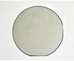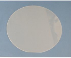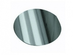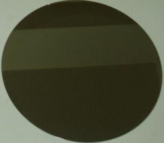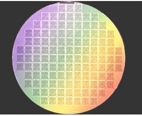
We provide custom thin film (silicon carbide) SiC epitaxy on 6H or 4H substrates for the development of silicon carbide devices. SiC epi wafer is mainly used for Schottky diodes, metal-oxide semiconductor field-effect transistors, junction field effect transistors, bipolar junction transistors, thyristors, GTO, and insulated gate bipolar.
SiC(Silicon Carbide) Epitaxy
We provide custom thin film (silicon carbide) SiC epitaxy on 6H or 4H substrates for the development of silicon carbide devices. SiC epi wafer is mainly used for Schottky diodes, metal-oxide semiconductor field-effect transistors, junction field effect transistors, bipolar junction transistors, thyristors, GTO, and insulated gate bipolar.
|
Items |
Specification |
Typical Value |
|
Poly-type |
4H |
— |
|
Off-orientation toward |
4 deg-off |
— |
|
<11 2(_) 0> |
||
|
Conductivity |
n-type |
— |
|
Dopant |
Nitrogen |
— |
|
Carrier Concentration |
5E15-2E18 cm-3 |
— |
|
Tolerance |
± 25% |
± 15% |
|
Uniformity |
2”(50.8mm)< 10% |
7% |
|
3”(76.2mm)< 20% |
10% |
|
|
4” (100mm)< 20% |
15% |
|
|
Thickness Range |
5-15 μm |
— |
|
Tolerance |
± 10% |
± 5% |
|
Uniformity |
2”< 5% |
2% |
|
3”< 7% |
3% |
|
|
4”< 10% |
5% |
|
|
Large Point Defects |
2”< 30 |
2”< 15 |
|
3”< 60 |
3”< 30 |
|
|
4”< 90 |
4”< 45 |
|
|
Epi Defects |
≤20 cm-2 |
≤10 cm-2 |
|
Step Bunching |
≤2.0nm (Rq) |
≤1.0nm (Rq) |
|
(Roughness) |
Notes:
• 2 mm edge exclusion for 50.8 and 76.2 mm, 3 mm edge exclusion for 100.0 mm
• Average of all measurement points for thickness and carrier concentration (see pg. 5)
• N-type epi layers <20 microns are preceeded by n-type, 1E18, 0.5 micron buffer layer
• Not all doping densities are available in all thicknesses
• Uniformity:standard deviation(σ)/average
• Any special requirement on the epi-parameter is on request
Test Methods
No.1. Carrier concentration:Net doping is determined as an average value across the afer using Hg probe CV.
No.2. Thickness: Thickness is determined as an average value across the wafer using FTIR.
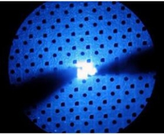
No.3.Large point defects: Microscopic inspection performed at 100X, on an Olympus Optical Microscope, or comparable.
No.4. Epi Defects Inspection performed under KLA-Tencor Candela CS20 Optical Surface Analyzer.
No.5. Step bunching: Step bunching and Roughness are scaned by AFM (atomic force microscope) on a 10μm x10μm area
Large Point Defects Descriptions
Defects which exhibit a clear shape to the unassisted eye and are > 50microns across. These features include spikes, adherent particles, chips andcraters. Large point defects less than 3 mm apart count as one defect.
Epitaxy Defect Descriptions
D1. 3C Inclusions
Regions where step-ow was interrupted during epi layer growth. Typicalregions are generally triangular although more rounded shapes are sometimesseen. Count once per occurrence. Two inclusions within 200 microns count asone.
D2. Comet Tails
Comet tails have a discrete head and trailing tail. These features are alignedparallel to the major at. Usually, all comet tails tend to be of the same length. Count once per occurrence. Two comet tails within 200 microns count as one.
D3. Carrots
Similar to comet tails in appearance except they are more angular and lack adiscrete head. If present, these features are aligned parallel to the major at. Usually, any carrots present tend to be of the same length. Count once peroccurrence. Two carrots within 200 microns count as one.
D4. Particles
Particles have the appearance of eyes and if present are usually concentratedat the wafer edges and not within the specied area. If present, count once peroccurrence. Two particles within 200 microns count as one.
D5. Silicon droplets
Silicon droplets can appear as either small mounds or depressions in the wafersurface. Normally absent, but if present are largely concentrated at perimeterof wafer. If present, estimate the % of specied area affected.
D6. Downfall
Adherent particles droped during Epi growth.
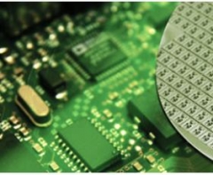
Application of SiC epitaxial wafer
Power factor correction(PFC)
PV inverter and UPS(Uninterrupted power supplies) inverters
Motor drives
Output rectification
Hybrid or electric vehicles
SiC Schottky diode with 600V, 650V, 1200V, 1700V, 3300V is available.
PAM-XIAMEN offers semiconductor silicon carbide wafers,6H SiC and 4H SiC in different quality grades for researcher and industry manufacturers. We has developed SiC crystal growth technology and SiC crystal wafer processing technology,established a production line to manufacturer SiC substrate,Which is applied in GaN epitaxy device,power devices,hi1
PAM-XIAMEN is able to offer the following SiC reclaim wafer services.
Due to SiC physical and electronic properties,Silicon Carbide based device are well suitable for short wavelength optoelectronic, high temperature, radiation resistant, and high-power/high-frequency electronic devices,compared with Si and GaAs based device.
PAM offers semiconductor materials,single crystal (Ge)Germanium Wafer grown by VGF / LEC
PAM-XIAMEN Offers Dummy Wafer / Test Wafer / Monitor Wafer
CZ-Silicon The heavily/lightly-doped CZ mono-crystalline silicon is suitable for producing various integrated circuits (IC), diodes, triodes, green-energy solar panel. The special elements (such as Ga, Ge) can be added to produce the high-efficiency, radiation-resistant and anti-degenerating solar cell materials for special components.
PAM-XIAMEN's GaN(gallium nitride)-based LED epitaxial wafer is for ultra high brightness blue and green light emitting diodes (LED) and laser diodes (LD) application.
Xiamen Powerway offers InP wafer - Indium Phosphide which are grown by LEC(Liquid Encapsulated Czochralski) or VGF(Vertical Gradient Freeze) as epi-ready or mechanical grade with n type, p type or semi-insulating in different orientation(111)or(100).
 Contact Information
 luna@powerwaywafer.compowerwaymaterial@gmail.com
  +86-592-5601 404