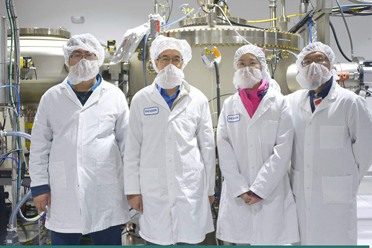
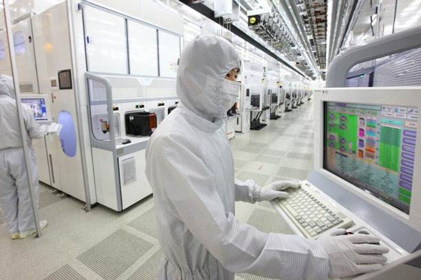
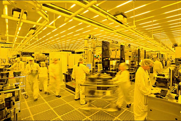
About Us
Before 1990, we are stated owned condensed matter physics research center. In 1990, center launched Xiamen Powerway Advanced Material Co., Ltd (PAM-XIAMEN), now it is a leading manufacturer of compound semiconductor material in China.
PAM-XIAMEN develops advanced crystal growth and epitaxy technologies, range from the first generation Germanium wafer, second generation Gallium Arsenide with substrate growth and epitaxy on III-V silicon doped n-type semiconductor materials based on Ga, Al, In, As and P grown by MBE or MOCVD, to the third generation: Silicon carbide and Gallium Nitride for LED and power device application.
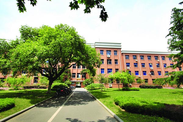
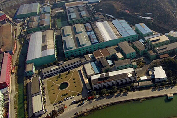
Quality is our first priority. PAM-XIAMEN has been ISO9001:2008 certified and awarded honors from China General Administration of Quality Supervision, Inspection and Quarantine. We have owns and shares four modern factories, which can provide quite a big range of qualified products to meet different needs of our customers.
History of PAM-XIAMEN
Before1990
We are stated owned condensed matter physics research center

Year1990
Xiamen Powerway Advanced Material Co.,Ltd(PAM-XIAMEN) founded. PAM-XIAMEN develops advanced crystal growth and epitaxy technologies, manufacturing processes, engineered substrates and semiconductor devices.

Year2001
PAM-XIAMEN has established production line of Semiconductor materials-Germanium Material and Wafers.

Year2004
PAM-XIAMEN launched research and development of silicon carbide material. after three years, the company established a production line to manufacturer Silicon carbide substrate of polytype 4H and 6H in different quality grades for researcher and industry manufacturers, which is applied in GaN epitaxy device, power devices,high-temperature device and optoelectronic Devices.

Year2007
PAM-XIAMEN develops and manufactures compound semiconductor substrates-gallium arsenide material, and provide epi wafer service.

Year2009
PAM-XIAMEN has established the manufacturing technology for Gallium Nitride material along with epitaxial wafers.

Year2011
Commercial CdZnTe material are on mass production, which is a new semiconductor, which enables to convert radiation to electron effectively, it is mainly used in infrared thin-film epitaxy substrate, X-ray and γ-ray detection, laser optical modulation, high-performance solar cells and other high-tech field.
Do You Want To Learn More?
If you would like a quotation or more information about our product,Please Contact Us Now!
 Contact Information
 luna@powerwaywafer.compowerwaymaterial@gmail.com
  +86-592-5601 404


