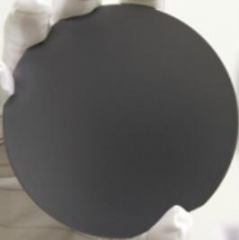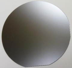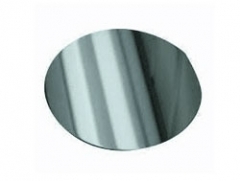
Xiamen Powerway offers InP wafer - Indium Phosphide which are grown by LEC(Liquid Encapsulated Czochralski) or VGF(Vertical Gradient Freeze) as epi-ready or mechanical grade with n type, p type or semi-insulating in different orientation(111)or(100).
Xiamen Powerway offers InP wafer - Indium Phosphide which are grown by LEC(Liquid Encapsulated Czochralski) or VGF(Vertical Gradient Freeze) as epi-ready or mechanical grade with n type, p type or semi-insulating in different orientation(111)or(100).
Indium phosphide (InP) is a binary semiconductor composed of indium and phosphorus. It has a face-centered cubic ("zinc blende") crystal structure, identical to that of GaAs and most of the III-V semiconductors.Indium phosphide can be prepared from the reaction of white phosphorus and indium iodide[clarification needed] at 400 °C.,[5] also by direct combination of the purified elements at high temperature and pressure, or by thermal decomposition of a mixture of a trialkyl indium compound and phosphide. InP is used in high-power and high-frequency electronics[citation needed] because of its superior electron velocity with respect to the more common semiconductors silicon and gallium arsenide.
| Wafer Specification | |
| Item | Specifications |
| Wafer Diameter | 50.5±0.4mm |
| Crystal Orientation | (100)±0.1° |
| Thickness | 350±25um / 500±25um |
| Primary flat length | 16±2mm |
| Secondary flat length | 8±1mm |
| Surface Finish | P/E, P/P |
| Package | Epi-Ready,Single wafer container or CF cassette |
| Electrical and Doping Specification | ||||||
| Conduction Type | n-type | n-type | n-type | n-type | p-type | p-type |
| Dopant | Undoped | Iron | Tin | Sulphur | Zinc | Low Zinc |
| E.D.P cm-2 | ≤5000 | ≤5000 | ≤50000 | ≤1000 | ≤1000 | ≤5000 |
| Mobility cm² V-1s-1 | ≥4200 | ≥1000 | 2500-750 | 2000-1000 | Not Specified | Not Specified |
| Carrier Concentration cm-3 | ≤1016 | Semi-Insulating | (7-40)*1017 | (1-10)*1018 | (1-6)*1018 | (1-6)*101 |
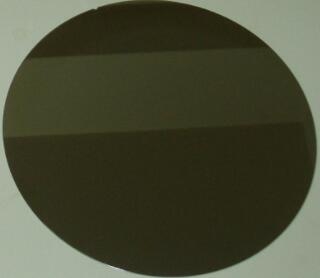
Xiamen Powerway offers InSb wafer - Indium antimonide which are grown by LEC(Liquid Encapsulated Czochralski) as epi-ready or mechanical grade with n type, p type or semi-insulating in different orientation(111)or(100).
Xiamen Powerway offers InAs wafer - Indium arsenide which are grown by LEC(Liquid Encapsulated Czochralski) as epi-ready or mechanical grade with n type, p type or semi-insulating in different orientation(111)or(100).
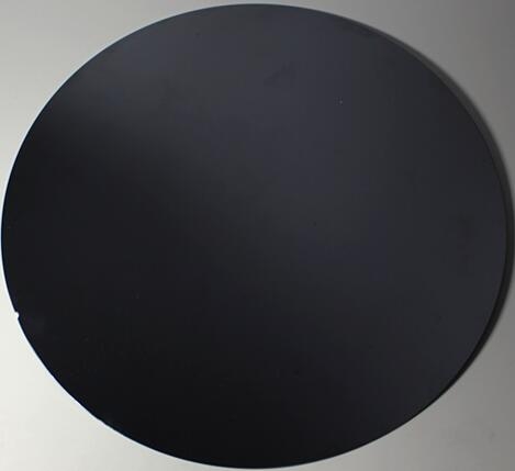
Xiamen Powerway offers GaP wafer - gallium Phosphide which are grown by LEC(Liquid Encapsulated Czochralski) as epi-ready or mechanical grade with n type, p type or semi-insulating in different orientation(111)or(100).
Xiamen Powerway offers GaSb wafer - gallium antimonide which are grown by LEC(Liquid Encapsulated Czochralski) as epi-ready or mechanical grade with n type, p type or semi-insulating in different orientation(111)or(100)
Xiamen Powerway offers InAs wafer - Indium arsenide which are grown by LEC(Liquid Encapsulated Czochralski) as epi-ready or mechanical grade with n type, p type or semi-insulating in different orientation(111)or(100).
CZ-Silicon The heavily/lightly-doped CZ mono-crystalline silicon is suitable for producing various integrated circuits (IC), diodes, triodes, green-energy solar panel. The special elements (such as Ga, Ge) can be added to produce the high-efficiency, radiation-resistant and anti-degenerating solar cell materials for special components.
We are manufacturing various types of epi wafer III-V silicon doped n-type semiconductor materials based on Ga, Al, In, As and P grown by MBE or MOCVD. We supply custom structures to meet customer specifications.please contact us for more information.
PAM-XIAMEN offers semiconductor silicon carbide wafers,6H SiC and 4H SiC in different quality grades for researcher and industry manufacturers. We has developed SiC crystal growth technology and SiC crystal wafer processing technology,established a production line to manufacturer SiC substrate,Which is applied in GaN epitaxy device,power devices,hi1
 Contact Information
 luna@powerwaywafer.compowerwaymaterial@gmail.com
  +86-592-5601 404