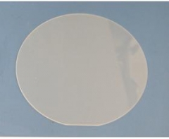
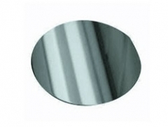
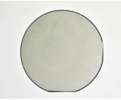
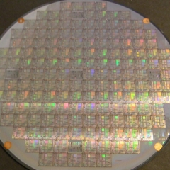
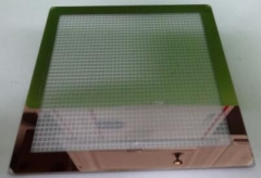
The etching wafer has the characteristics of low roughness, good glossiness and relatively low cost, and directly substitutes the polished wafer or epitaxial wafer which has relatively high cost to produce the electronic elements in some fields, to reduce the costs. There are the low-roughness, low-reflectivity and high-reflectivity etching wafers.
Etching wafer
The etching wafer has the characteristics of low roughness, good glossiness and relatively low cost, and directly substitutes the polished wafer or epitaxial wafer which has relatively high cost to produce the electronic elements in some fields, to reduce the costs. There are the low-roughness, low-reflectivity and high-reflectivity etching wafers.
Our advantages at a glance
1.Advanced epitaxy growth equipment and test equipment.
2.Offer the highest quality with low defect density and good surface roughness.
3.Strong research team support and technology support for our customers
FZ etching wafers Specifications
|
Type |
Conduction type |
Orientation |
Diameter scope(mm) |
Resistivity scope(Ω cm) |
Geometric parameter,graininess,surface metal |
|
FZ |
N&P |
<100>&<111> |
76.2-200 |
>1000 |
T≥180(um)TTV≤2(um)TIR≤2(um)the maximum reflectivity could be 90% |
|
NTDFZ |
N |
<100>&<111> |
76.2-200 |
30-800 |
|
|
CFZ |
N&P |
<100>&<111> |
76.2-200 |
1-50 |
|
|
GDFZ |
N&P |
<100>&<111> |
76.2-200 |
0.001-300 |
CZ etching wafers Specifications
|
Type |
Conduction type |
Orientation |
Diameter scope(mm) |
Resistivity scope(Ω cm) |
Geometric parameter,graininess,surface metal |
|
MCZ |
N&P |
<100> <110>&<111> |
76.2-200 |
1-300 |
T≥180(um)TTV≤2(um)TIR≤2(um)the maximum reflectivity could be 90% |
|
CZ |
N&P |
<100> <110>&<111> |
76.2-200 |
1-300 |
|
|
MCZ heavily doped |
N&P |
<100> <110>&<111> |
76.2-200 |
0.001-1 |
FZ-Silicon The mono-crystalline silicon with the characteristics of low foreign-material content, low defect density and perfect crystal structure is produced with the float-zone process; no foreign material is introduced during the crystal growth. The FZ-Silicon conductivity is usually above 1000 Ω-cm, and the FZ-Silicon is mainly used to produce 1
PAM-XIAMEN Offers Dummy Wafer / Test Wafer / Monitor Wafer
CZ-Silicon The heavily/lightly-doped CZ mono-crystalline silicon is suitable for producing various integrated circuits (IC), diodes, triodes, green-energy solar panel. The special elements (such as Ga, Ge) can be added to produce the high-efficiency, radiation-resistant and anti-degenerating solar cell materials for special components.
Silicon Epitaxial Wafer(Epi Wafer) is a layer of single crystal silicon deposited onto a single crystal silicon wafer(note: it is available to Grow a layer of poly crystalline Silicon layer on top of a highly doped Singly crystalline Silicon wafer,but it needs buffer layer (such as oxide or poly-Si) in between the bulk Si substrate and the top epit1
FZ polished wafers, mainly for the production of silicon rectifier (SR), silicon controlled rectifier (SCR), Giant Transistor (GTR), thyristor (GRO)
PAM-XIAMEN offers semiconductor silicon carbide wafers,6H SiC and 4H SiC in different quality grades for researcher and industry manufacturers. We has developed SiC crystal growth technology and SiC crystal wafer processing technology,established a production line to manufacturer SiC substrate,Which is applied in GaN epitaxy device,power devices,hi1
PAM-XIAMEN Offers photoresist plate with photoresist We can offer Nanolithography (photolithography):Surface preparation, Photoresist apply, Soft bake, Alignment, Exposure, Development,Hard bake, Develop inspect, Etch, Photoresist removal(strip), Final inspection.
PAM-XIAMEN Offers Photomasks A photo mask is a thin coating of masking material supported by a thicker substrate, and the masking material absorbs light to varying degrees and can be patterned with a custom design. The pattern is used to modulate light and transfer the pattern through the process of photolithography which is the fundamental process1
 Contact Information
 luna@powerwaywafer.compowerwaymaterial@gmail.com
  +86-592-5601 404