PAM-XIAMEN Offers Photomasks
A photo mask is a thin coating of masking material supported by a thicker substrate, and the masking material absorbs light to varying degrees and can be patterned with a custom design. The pattern is used to modulate light and transfer the pattern through the process of photolithography which is the fundamental process used to build almost all of today’s digital devices.
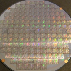
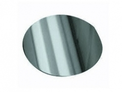
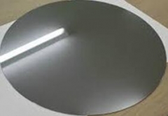
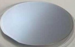
Photo Mask
PAM-XIAMEN Offers Photomasks
A photo mask is a thin coating of masking material supported by a thicker substrate, and the masking material absorbs light to varying degrees and can be patterned with a custom design. The pattern is used to modulate light and transfer the pattern through the process of photolithography which is the fundamental process used to build almost all of today’s digital devices.
What is a Photomask
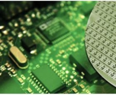
A photomask is an opaque plate with holes or transparencies that allow light to shine through in a defined pattern. They are commonly used in photolithography. Lithographic photomasks are typically transparent fused silica blanks covered with a pattern defined with a chrome metal-absorbing film. Photomasks are used at wavelengths of 365 nm, 248 nm, and 193 nm. Photomasks have also been developed for other forms of radiation such as 157 nm, 13.5 nm (EUV), X-ray, electrons, and ions; but these require entirely new materials for the substrate and the pattern film. A set of photomask, each defining a pattern layer in integrated circuit fabrication, is fed into a photolithography stepper or scanner, and individually selected for exposure. In double patterning techniques, a photomask would correspond to a subset of the layer pattern. In photolithography for the mass production of integrated circuit devices, the more correct term is usually photoreticle or simply reticle. In the case of a photomask, there is a one-to-one correspondence between the mask pattern and the wafer pattern. This was the standard for the 1:1 mask aligners that were succeeded by steppers and scanners with reduction optics. As used in steppers and scanners, the reticle commonly contains only one layer of the chip. (However, some photolithography fabrications utilize reticles with more than one layer patterned onto the same mask). The pattern is projected and shrunk by four or five times onto the wafer surface. To achieve complete wafer coverage, the wafer is repeatedly “stepped” from position to position under the optical column until full exposure is achieved. Features 150 nm or below in size generally require phase-shifting to enhance the image quality to acceptable values. This can be achieved in many ways. The two most common methods are to use an attenuated phase-shifting background film on the mask to increase the contrast of small intensity peaks, or to etch the exposed quartz so that the edge between the etched and unetched areas can be used to image nearly zero intensity. In the second case, unwanted edges would need to be trimmed out with another exposure. The former method is attenuated phase-shifting, and is often considered a weak enhancement, requiring special illumination for the most enhancement, while the latter method is known as alternating-aperture phase-shifting, and is the most popular strong enhancement technique. As leading-edge semiconductor features shrink, photomask features that are 4× larger must inevitably shrink as well. This could pose challenges since the absorber film will need to become thinner, and hence less opaque. A recent study by IMEC has found that thinner absorbers degrade image contrast and therefore contribute to line-edge roughness, using state-of-the-art photolithography tools. One possibility is to eliminate absorbers altogether and use “chromeless” masks, relying solely on phase-shifting for imaging. The emergence of immersion lithography has a strong impact on photomask requirements. The commonly used attenuated phase-shifting mask is more sensitive to the higher incidence angles applied in “hyper-NA” lithography, due to the longer optical path through the patterned film.
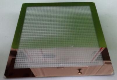
Mask Materials -Difference between Quartz and Soda Lime Glass:
The most common types of glass for manufacturing masks are Quartz and Soda Lime. Quartz is more expensive, but has the advantage of a much lower coefficient of Thermal Expansion (which means it expands less if the mask gets warm during use) and is also transparent at deeper Ultraviolet (DUV) wavelengths, where Soda Lime glass is opaque. Quartz needs to be used where the wavelength being used to expose the mask is less than or equal to 365nm (i-line).A photolithography mask is an opaque plate or film with transparent areas that allow light to shine through in a defined pattern. They are commonly used in photolithography processes, but are also used in many other applications by a wide range of industries and technologies. It exists different kind of mask for different application namely based on the resolution needed.
For more product detail, please contact us at luna@powerwaywafer.com or powerwaymaterial@gmail.com.
1X Master Mask
1X Master Mask Dimensions and Substrate Materials
|
Product |
Dimensions |
Substrate Materials |
|
1X Master |
4” X4” X0.060” or 0.090” |
Quartz and Soda Lime |
|
5” X5” X0.090” |
Quartz and Soda Lime |
|
|
6” X6” X0.120” or 0.250” |
Quartz and Soda Lime |
|
|
7” X7” X0.120” or 0.150” |
Quartz and Soda Lime |
|
|
7.25” Round X 0.150” |
Quartz |
|
|
9”X9”X0.120” or 0.190” |
Quartz and Soda Lime |
Common Specifications for 1X Master Masks(Quartz Material)
|
CD Size |
CD Mean-to-Nominal |
CD Uniformity |
Registration |
defect Size |
|
2.0 um |
≤0.25 um |
≤0.25 um |
≤0.25 um |
≥2.0 um |
|
4.0 um |
≤0.30 um |
≤0.30 um |
≤0.30 um |
≥3.5 um |
Common Specification for 1X Master Masks(Soda Lime Material)
|
CD Size |
CD Mean-to-Nominal |
CD Uniformity |
Registration |
defect Size |
|
≤4 um |
≤0.25 um |
———— |
≤0.25 um |
≥3.0 um |
|
>4 um |
≤0.30 um |
———— |
≤0.45 um |
≥5.0 um |
UT1X Mask
UT1X Mask Dimensions and Substrate Materials
|
Product |
Dimensions |
Substrate Material |
|
UT1X |
3″ X5″ X0.090″ |
Quartz |
|
5″ X5″ X0.090″ |
Quartz |
|
|
6″ X6″X0.120″ or 0.250″ |
Quartz |
Common Specifications for UT1X Masks
|
CD Size |
CD Mean-to-Nominal |
CD Uniformity |
Registration |
defect Size |
|
1.5 um |
≤0.15 um |
≤0.15 um |
≤0.15 um |
≥0.50 um |
|
3.0 um |
≤0.20 um |
≤0.20 um |
≤0.20 um |
≥0.60 um |
|
4.0 um |
≤0.25 um |
≤0.25 um |
≤0.20 um |
≥0.75 um |
Standard Binary Masks
Standard Binary Mask Dimensions and Substrate Materials
|
Product |
Dimensions |
Substrate Materials |
|
2X |
6″X 6″ X0.250″ |
Quartz |
|
2.5X |
||
|
4X |
||
|
5X |
5″ X5″ X0.090″ |
Quartz |
|
6″ X6″ X0.250″ |
Quartz |
Common Specifications for Standard Binary Masks
|
CD Size |
CD Mean-to-Nominal |
CD Uniformity |
Registration |
defect Size |
|
2.0 um |
≤0.10 um |
≤0.15 um |
≤0.10 um |
≥0.50 um |
|
3.0 um |
≤0.15 um |
≤0.15 um |
≤0.15 um |
≥0.75 um |
|
4.0 um |
≤0.20 um |
≤0.20 um |
≤0.20 um |
≥1.00 um |
Medium Area Masks
Medium Area Mask Dimensions and Materials
|
Product |
Dimensions |
Substrate Materials |
|
1X |
9″ X9″ 0.120″ |
Quartz Soda Lime(both Chrome and Iron Oxide absorbers available) |
|
9″ X9″ 0.190″ |
Quartz |
Common Specifications for Medium Area Masks(Quartz Material)
|
CD Size |
CD Mean-to-Nominal |
CD Uniformity |
Registration |
defect Size |
|
0.50 um |
≤0.20 um |
———— |
≤0.15 um |
≥1.50 um |
Common Specifications for Medium Area Masks(Soda Lime Material)
|
CD Size |
CD Mean-to-Nominal |
CD Uniformity |
Registration |
defect Size |
|
10 um |
≤4.0 um |
———— |
≤4.0 um |
≥10 um |
|
4 um |
≤2.0 um |
———— |
≤1.0 um |
≥5 um |
|
2.5 um |
≤0.5 um |
———— |
≤0.75 um |
≥3 um |
PAM-XIAMEN Offers photoresist plate with photoresist We can offer Nanolithography (photolithography):Surface preparation, Photoresist apply, Soft bake, Alignment, Exposure, Development,Hard bake, Develop inspect, Etch, Photoresist removal(strip), Final inspection.
Cadmium Zinc Telluride (CdZnTe or CZT) is a new semiconductor, which enables to convert radiation to electron effectively, it is mainly used in infrared thin-film epitaxy substrate,X-ray detectors and Gamma-ray detectors, laser optical modulation, high-performance solar cells and other high-tech fields.
Silicon Epitaxial Wafer(Epi Wafer) is a layer of single crystal silicon deposited onto a single crystal silicon wafer(note: it is available to Grow a layer of poly crystalline Silicon layer on top of a highly doped Singly crystalline Silicon wafer,but it needs buffer layer (such as oxide or poly-Si) in between the bulk Si substrate and the top epit1
We provide custom thin film (silicon carbide) SiC epitaxy on 6H or 4H substrates for the development of silicon carbide devices. SiC epi wafer is mainly used for Schottky diodes, metal-oxide semiconductor field-effect transistors, junction field effect transistors, bipolar junction transistors, thyristors, GTO, and insulated gate bipolar.
Due to SiC physical and electronic properties,Silicon Carbide based device are well suitable for short wavelength optoelectronic, high temperature, radiation resistant, and high-power/high-frequency electronic devices,compared with Si and GaAs based device.
CZ-Silicon The heavily/lightly-doped CZ mono-crystalline silicon is suitable for producing various integrated circuits (IC), diodes, triodes, green-energy solar panel. The special elements (such as Ga, Ge) can be added to produce the high-efficiency, radiation-resistant and anti-degenerating solar cell materials for special components.
The etching wafer has the characteristics of low roughness, good glossiness and relatively low cost, and directly substitutes the polished wafer or epitaxial wafer which has relatively high cost to produce the electronic elements in some fields, to reduce the costs. There are the low-roughness, low-reflectivity and high-reflectivity etching wafers.
Xiamen Powerway offers GaSb wafer - gallium antimonide which are grown by LEC(Liquid Encapsulated Czochralski) as epi-ready or mechanical grade with n type, p type or semi-insulating in different orientation(111)or(100)
 Contact Information
 luna@powerwaywafer.compowerwaymaterial@gmail.com
  +86-592-5601 404