We can offer 2" AlInP/GaAs epi wafer as follows:
2” AlInP epi layer: epi layer:1-3um,
GaAs substrate:2”size,orientation (100) or (110), n type or semi-insulating, thickness:300-500um, single side polished.
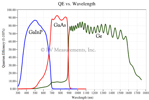
Example QE measurement of a triple-junction solar cell:
Source: semiconductorwafers.net
For more information, please visit our website:http://www.semiconductorwafers.net,
send us email at angel.ye@powerwaywafer.com or powerwaymaterial@gmail.com.
 Contact Information
 luna@powerwaywafer.compowerwaymaterial@gmail.com
  +86-592-5601 404


