Thermal Grade Diamand Wafers and Slices
Diamond exhibits the highest thermal conductivity among all materials. Its thermal
conductivity is up to 2000 W/mK which is higher a lot than that of copper. Therefore
diamond wafers and slices become more and more popular in thermal management as
heatspreaders,heatsinks, lithographically patterned metallization, electrical isolation
between top and bottom metallization, stress relieving slits for stress free mounting etc.
CVD diamond heat spreaders in various shapes,and the typical parameters are as
follows:
Material thermal conductivity >1000 W/mK
Diameter Up to 70mm
Surface Polished, lapping, as-cut
Thickness 100 - 1500 µm
Young's modulus 1000-1100Gpa
Density 3.5g/cm3
Optical grade diamond wafers
Optical grade diamond wafers are used as window for infrared beam splitters, lenses for
terahertz spectroscopy and CO2 laser surgery,Brewster Windows for multi-spectral
applications such as free electron lasers, multi-wavelength IR lasers or terahertz optical
systems,for Units attenuated total reflection) spectroscopy,for diamond Liquid Cells.
Large Sized Diamond Substrate
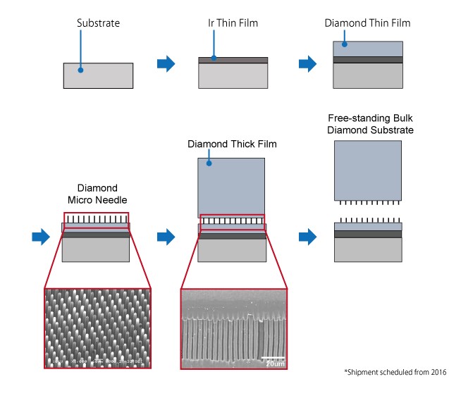
Long known as one of the top industrial jewel parts suppliers, we have been continuing to improve its jewel substrate manufacture technology when it mass produced 14mm*14mm single crystal diamond substrates for post-Si semiconductors that build optical parts, heat spreader, audio parts and quantum computer. At present, we are able to manufacture substrates in the size of around 1 inch square with the exclusive, patented microneedle growth technology enabling stable production of crack-free large diamond substrate. Carrying on with the technology, we promised to scale up the size of its substrate products to up to 50mm*50mm (2 inch square).
Keywords: Diamond wafers,Diamond wafer
Source: semiconductorwafers.net
For more information, please visit our website:http://www.semiconductorwafers.net,
send us email at angel.ye@powerwaywafer.com or powerwaymaterial@gmail.com.
 Contact Information
 luna@powerwaywafer.compowerwaymaterial@gmail.com
  +86-592-5601 404


