Abstract
For solar cell application, the stability of interface passivation quality to in-field conditions is crucial. We have performed an experiment to test the resilience of different aluminium oxide based passivation schemes to illumination at 75 °C. Different thermal treatments to activate the passivation and/or simulate contact firing were performed before light soaking. The experiment was performed on 1 Ωcm float-zone silicon of both p- and n-type doping. The study demonstrates that good passivation quality can be achieved both by atomic layer deposition and by PECVD and that addition of silicon nitride capping layers greatly enhances thermal stability. On p-type wafers a severe but temporary degradation of the electrical quality of the wafer bulk was observed during the first hours upon application of such capping layers. Besides this effect, reasonable temporal stability of the effective lifetime was observed for p-type samples while n-type samples featured excellent long-term stability.
Keywords:float zone silicon;aluminum oxide passivation;stability;light soaking
1. Introduction
Recent improvements of the efficiency of industrially feasible solar cell concepts have been driven by
improvements of the material bulk quality and reduction of recombination losses at the surfaces. This was supported
by the emergence of passivation schemes based on aluminium oxide for industrial application due to their good
passivation properties. The good passivation quality of aluminium oxide layers is well established in literature and
demonstrated by a multitude of studies, e.g. [1] and references therein. Studies concerning the stability of
passivation schemes usually focus on one system and/or one stress factor such as dark storage, illumination or damp
heat testing conditions [2-4]. To generalize the previous findings we have performed a study comparing multiple
different schemes at a stress factor combination that occurs upon photovoltaic module operation: illumination at
elevated temperature.
Nomenclature
Al2O3 stoichiometric aluminium oxide layers deposited by P-ALD
AlOx aluminium oxide layers deposited by PECVD
FZ float-zone
LeTID Light and elevated temperature induced degradation
P-ALD plasma-activated atomic layer deposition
PECVD plasma-enhanced chemical vapour deposition
PLI photoluminescence imaging
RTP rapid thermal processing
SRV surface recombination velocity
2. Experiment
2.1. Sample preparation All experiments were performed on four inch float-zone (FZ) silicon wafers. After wet chemical cleaning, an oxidation treatment at 1050 °C was performed to stabilize the wafer bulk quality, as suggested by Grant et al. [5]. The resulting silicon oxide layer was subsequently etched off. To demonstrate whether the thermal treatment affected the experiment, a reference sample group was not subjected to it. The investigated aluminium oxide layers of 20 or 30 nm thickness were deposited on both wafer sides either by plasma-activated atomic layer deposition (P-ALD) at 230 °C or by plasma-enhanced chemical vapour deposition (PECVD) at 300 °C. The common application of aluminium oxide layers in industrial environment is thin layers capped by further dielectric layers. These layers usually provide additional functions such as optical improvements or simplified structuration. Layers of PECVD deposited silicon nitride a-SiNx were also shown to be beneficial for the stability of aluminium oxide passivation layers to thermal treatments, e.g. [6, 7]. Therefore, for a part of the sample groups 100 nm of a-SiNx (refractive index 2) were deposited on top the aluminium oxide layers. After deposition, the passivation layers were activated by a variety of thermal treatments resembling potential treatments in solar cell processing. The samples were either annealed in forming gas at 425 °C, in ambient air on a hotplate at 450 °C or in a nitrogen atmosphere in a rapid thermal processing (RTP) furnace at 650 to 900 °C. The uncertainty concerning the actual sample temperature for the latter process is estimated to be in a range of Tset ± 15 K from thermocouple measurements.
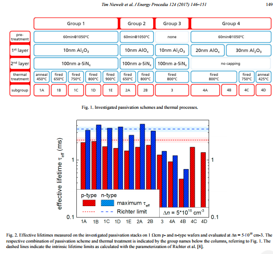
A wide range of passivation scheme and thermal process combinations was investigated in the study. An overview of the investigated variations is given in Fig. 1.
2.2. Testing conditions and characterization Measurements of the effective minority charge carrier lifetime τeff on symmetrical lifetime samples provide a measure for the recombination in the wafer bulk and at the interfaces to the surface passivation. A Sinton Instruments WCT-120 lifetime tester was used to measure τeff in a 4 cm diameter region around the middle of the
sample. Lifetimes were evaluated at fixed minority charge carrier density of 5×1015 cm-3 for both doping types.
Recombination activity in the wafer and changes of the surface passivation quality can easily be resolved at this
injection level and measurement in the wafer centre minimizes the influence of handling damages.
The stability of the studied passivation schemes to illumination at elevated temperature was performed by 1 sun
equivalent halogen lamp illumination at 75 °C. Lifetime measurements were performed ex situ, i.e. the samples were
removed from the temperature-controlled sample stage.
Temperatures in the range of 75 °C can occur in in-field module operation under intense illumination. Such
conditions obviously do not apply continuously. However, we expect these conditions to accelerate and intensify
possible degradation effects while – hopefully – no effects are triggered that would not occur in actual application. It
should be noted that the used halogen lamp illumination featured a smaller share of UV wavelengths than the solar
spectrum. On the other hand, this part of the spectrum is often absorbed in conventional module glass and solar cell
encapsulation materials.
3. Results
3.1. Passivation quality
An overview of the best measured τeff values of the sample groups introduced in Fig. 1 are shown in Fig. 2. The
measured τeff on the samples demonstrates that the different passivation schemes and thermal processes result in
different passivation quality. We observe that both deposition techniques for aluminium oxide can provide excellent
passivation when an a-SiNx capping layer is deposited on top. The investigated samples of groups 1 and 2 feature τeff
values close to the parameterization of the intrinsic limit by Richter et al. [8]. Some n-type samples even exceed the
parameterization, indicating an outstanding passivation performance. Some of the p-type samples are slightly
affected by iron contamination introduced during wet-chemical processing, which causes a small decrease in
lifetime. Besides the effects induced by iron, an improvement in τeff is observed on some samples upon illumination
at 75 °C, indicating an improvement of the interface parameters over time. Samples that did not undergo the
1050 °C oxidation step (group 3) exhibit lower τeff than samples featuring the same surface passivation after the
thermal pre-treatment. The samples that do not feature an a-SiNx capping layer (group 4) result in a lower lifetime
level, demonstrating the helpfulness of such layers.
3.2. Activation of bulk defects in p-type FZ silicon.
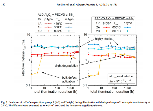
We observe that several p-type samples from groups 1 to 3 (i.e. featuring a capping layer) show a degradation
by a recovery of τeff upon illumination at 75 °C in the first few hours. A similar effect was observed by
Sperber et al. [9] and examples are shown in Fig. 3. Depending on the firing temperature, we observe the temporary
degradation to be severe. Samples fired at high temperatures exhibit low injection lifetimes as low as 30 µs in the
curve minimum, while samples fired at moderate temperatures show only slight degradation. A characteristic pattern
is seen in photoluminescence imaging and a room temperature re-passivation treatment conclusively demonstrates
the effect to be caused by recombination-active defects in the wafer bulk. A thorough investigation and discussion of
the effect can be found in Ref.
3.3. Long-term stability
The temporal evolutions of τeff measured on samples from groups 1 and 2 are shown in Fig. 3. The n-type
samples feature an excellent stability throughout the experiment. The progression of the p-type samples is
dominated by the bulk defects discussed in section 3.2 (and Ref. [10]) in the first ten to twenty hours. Afterwards,
the lifetimes are stable on a high level for 1000 hours, by a slight degradation. The samples passivated by
bare aluminium oxide layers (group 4) showed a slight but steady degradation of the measured τeff (not shown).
However, PL imaging revealed the degradation to originate from sample handling related surface damages of the
thin layers. Due to the lower overall lifetime level, we cannot exclude the effect observed on capped p-type samples
to occur on bare aluminium oxide layers, yet. The measured progressions of all sample groups and a detailed
discussion can be found in Ref.
4. Conclusion
We have performed an experiment with a variety of aluminium oxide based passivation schemes deposited on 1 Ωcm p- and n-type FZ silicon wafers. They were subjected to different thermal activation treatments to study the resulting passivation quality and its stability to illumination at elevated temperature. The measured effective lifetimes demonstrate that aluminium oxide layers can provide very good passivation quality. The measured lifetimes on some n-type samples even systematically exceed the current parameterization of intrinsic recombination given by Richter et al. [8]. This indicates excellent passivation quality and suggests the parameterization to be too conservative.
Stability tests were performed by halogen lamp illumination with one sun equivalent intensity at 75 °C for several thousand hours. Excellent stability of n-type samples passivated by aluminium oxide and protected by an a-SiNx capping layer was observed. P-type samples processed alike featured a significant but temporary degradation of bulk lifetime and a slight degradation for illumination durations exceeding 1000 hours. The experimental conditions (i.e. mostly the constant high temperature) result in a significant acceleration of effects when compared to in-field application. Therefore, the results simulate in-field application of several years and thus the observed degradation is not expected to be very harmful for module operation. However, the effect should be kept in mind for the interpretation of studies performed under such conditions, e.g. studies of LeTID or the stability of the stabilized BO defect state.
The long-term stability of the investigated passivation schemes is discussed in detail in Ref. [11]. The degradation is related to the formation of defects in the wafer bulk and is the main subject of Ref.
Acknowledgements
This work was supported by the German Federal Ministry for Economic Affairs and Energy BMWi and by the industry partners within the research cluster SolarLIFE under contract No. 0325763A. The authors are responsible for the content.
Source:ScienceDirect
For more information, please visit our website: http://www.semiconductorwafers.net,
send us email at angel.ye@powerwaywafer.com or powerwaymaterial@gmail.com.
 Contact Information
 luna@powerwaywafer.compowerwaymaterial@gmail.com
  +86-592-5601 404


