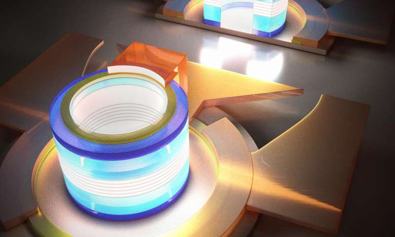
Schematic of the electrically pumped quantum dot micro-ring laser. Credit: Department of Electronic and Computer Engineering, HKUST
Decades ago, the Moore’s law predicted that the number of transistors in a dense integrated circuit doubles approximately every two years. This prediction was proved to be right in the past few decades, and the quest for ever smaller and more efficient semiconductor devices have been a driving force in breakthroughs in the technology.
With an enduring and increasing need for miniaturization and large-scale integration of photonic components on the silicon platform for data communication and emerging applications in mind, a group of researchers from the Hong Kong University of Science and Technology and University of California, Santa Barbara, successfully demonstrated record-small electrically pumped micro-lasers epitaxially grown on industry standard (001) silicon substrates in a recent study. A submilliamp threshold of 0.6 mA, emitting at the near-infrared (1.3?m) was achieved for a micro-laser with a radius of 5 μm. The thresholds and footprints are orders of magnitude smaller than those previously reported lasers epitaxially grown on Si.
Their findings were published in the prestigious journal Optica on August
“We demonstrated the smallest current injection QD lasers directly grown on industry-standard (001) silicon with low power consumption and high temperature stability,” said Kei May Lau, Fang Professor of Engineering and Chair Professor of the Department of Electronic & Computer Engineering at HKUST.
“The realization of high-performance micron-sized lasers directly grown on Si represents a major step toward utilization of direct III-V/Si epitaxy as an alternate option to wafer-bonding techniques as on-chip silicon light sources with dense integration and low power consumption.”
The two groups have been collaborating and has previously developed continuous-wave (CW) optically-pumped micro-lasers operating at room temperature that were epitaxially grown on silicon with no germanium buffer layer or substrate miscut. This time, they demonstrated record-small electrically pumped QD lasers epitaxially grown on silicon. “Electrical injection of micro-lasers is a much more challenging and daunting task: first, electrode metallization is limited by the micro size cavity, which may increase the device resistance and thermal impedance; second, the whispering gallery mode (WGM) is sensitive to any process imperfection, which may increase the optical loss,” said Yating Wan, a HKUST PhD graduate and now postdoctoral fellow at the Optoelectronics Research Group of UCSB.
“As a promising integration platform, silicon photonics need on-chip laser sources that dramatically improve capability, while trimming size and power dissipation in a cost-effective way for volume manufacturability. The realization of high-performance micron-sized lasers directly grown on Si represents a major step toward utilization of direct III-V/Si epitaxy as an alternate option to wafer-bonding techniques,” said John Bowers, Deputy Chief Executive Officer of AIM Photonics.
Source:PHYS
For more information, please visit our website: http://www.semiconductorwafers.net,
send us email at angel.ye@powerwaywafer.com or powerwaymaterial@gmail.com.
 Contact Information
 luna@powerwaywafer.compowerwaymaterial@gmail.com
  +86-592-5601 404


