SiC Reclaim Wafer & Processing
PAM-XIAMEN is able to offer the following SiC reclaim wafer services.
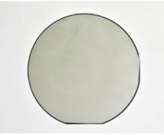
SiC Reclaim Wafer:
PAM-XIAMEN is able through is proprietry reclaim processes to offer a SiC reclaim wafer services to LED, RF or Power device manufacturers.Able to remove EPI, EPI GaN or device layers,and then polish the surface,till to an Epi ready state,which our customers can epi them again, to reduce the cost.We even can gurantee surface roughness <0.3nm as customer required.Each wafer is by CMP or lapped or etched to remove patterns, scratches and other defects. The result is a clean, high-quality wafer that is ready for polishing and cleaning. At the conclusion of the reclaim process, to verify the finished wafers fully comply with customer standards and specifications, we will do a final quality inspection before packaging.We put the reclaimed wafers into containers. The containers are double-bagged and labeled. As a final step, we provide a Certificate of Conformance and/or Analysis Certificate, as required, to verify product quality.
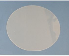
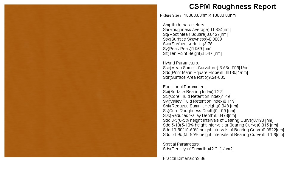
Below is AFM image after CMP as an example:
SiC Surface Preparation: PAM-XIAMEN has developed using it’s long experience in silicon carbide wafer cleaning a process,which is able to deliver clean low metallic contamination on new SiC substrates.
We provide custom thin film (silicon carbide) SiC epitaxy on 6H or 4H substrates for the development of silicon carbide devices. SiC epi wafer is mainly used for Schottky diodes, metal-oxide semiconductor field-effect transistors, junction field effect transistors, bipolar junction transistors, thyristors, GTO, and insulated gate bipolar.
PAM-XIAMEN offers semiconductor silicon carbide wafers,6H SiC and 4H SiC in different quality grades for researcher and industry manufacturers. We has developed SiC crystal growth technology and SiC crystal wafer processing technology,established a production line to manufacturer SiC substrate,Which is applied in GaN epitaxy device,power devices,hi1
Due to SiC physical and electronic properties,Silicon Carbide based device are well suitable for short wavelength optoelectronic, high temperature, radiation resistant, and high-power/high-frequency electronic devices,compared with Si and GaAs based device.
PWAM Develops and manufactures compound semiconductor substrates-gallium arsenide crystal and wafer.We has used advanced crystal growth technology,vertical gradient freeze(VGF) and GaAs wafer processing technology,established a production line from crystal growth, cutting, grinding to polishing processing and built a 100-class clean room for 1
PAM-XIAMEN Offers Dummy Wafer / Test Wafer / Monitor Wafer
FZ-Silicon The mono-crystalline silicon with the characteristics of low foreign-material content, low defect density and perfect crystal structure is produced with the float-zone process; no foreign material is introduced during the crystal growth. The FZ-Silicon conductivity is usually above 1000 Ω-cm, and the FZ-Silicon is mainly used to produce 1
PAM-XIAMEN provides CZT based detectors by solid-state detector technology for x-ray or gamma-ray,which has better energy resolution compared with scintillation crystal based detector, including CZT Planar Detector,CZT Pixilated Detector,CZT Co-Planar Gri
We provide custom thin film (silicon carbide) SiC epitaxy on 6H or 4H substrates for the development of silicon carbide devices. SiC epi wafer is mainly used for Schottky diodes, metal-oxide semiconductor field-effect transistors, junction field effect transistors, bipolar junction transistors, thyristors, GTO, and insulated gate bipolar.
 Contact Information
 luna@powerwaywafer.compowerwaymaterial@gmail.com
  +86-592-5601 404