PAM-XIAMEN's GaN(gallium nitride)-based LED epitaxial wafer is for ultra high brightness blue and green light emitting diodes (LED) and laser diodes (LD) application.
MOQ :
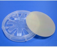
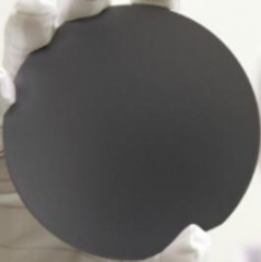
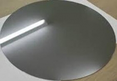
1GaN(gallium nitride) based LED Epitaxial Wafer
As LED wafer manufacturer,we offer LED wafer for LED and laser diodes (LD) application,such as For micro LED or ultra thin wafer or UV LED researches or LED manufacturers.it is by MOCVD with PSS or flat sapphire for LCD back light, mobile,electronic or UV(ultraviolet), with blue or green or red emission,including InGaN/GaN active area and AlGaN layers with GaN well/AlGaN barrier for different chip sizes.
GaN on Al2O3-2” epi wafer Specification(LED Epitaxial wafer)
|
UV LED: 365nm,405nm |
|
White: 445~460 nm |
|
Blue: 465~475 nm |
|
Green: 510~530 nm |
1. Growth Technique - MOCVD
2.Wafer diameter: 50.8mm
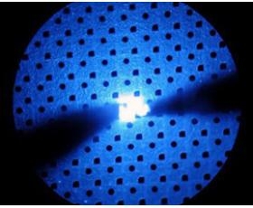
3.Wafer substrate material: Patterned Sapphire Substrate(Al2O3)
4.Wafer pattern size: 3X2X1.5μm
5.Wafer structure:
|
Structure layers |
Thickness(μm) |
|
p-GaN |
0.2 |
|
p-AlGaN |
0.03 |
|
InGaN/GaN(active area) |
0.2 |
|
n-GaN |
2.5 |
|
u- GaN |
3.5 |
|
Al2O3 (Substrate) |
430 |
6.Wafer parameters to make chips:
|
Item |
Color |
Chip Size |
Characteristics |
Appearance |
|
|
|
PAM1023A01 |
Blue |
10mil x 23mil |
|
|
Lighting |
|
|
Vf = 2.8~3.4V |
LCD backlight |
|||||
|
Po = 18~25mW |
Mobile appliances |
|||||
|
Wd = 450~460nm |
Consumer electronic |
|||||
|
PAM454501 |
Blue |
45mil x 45mil |
Vf = 2.8~3.4V |
|
General lighting |
|
|
Po = 250~300mW |
LCD backlight |
|||||
|
Wd = 450~460nm |
Outdoor display |
*If you need to know more detail information of Blue LED Chip, please contact with our sales departments
7.Application of LED epitaixal wafer:
Lighting
LCD back light
Mobile appliances
Consumer electronic
PAM-XIAMEN's GaN-based epitaxial wafers(Epi Wafer) is for ultra high brightness blue and green light emitting diodes (LED)
GaAs(Gallium arsenide)based LED Wafer:
Regarding GaAs LED wafer, they are grown by MOCVD,see below wavelength of GaAs LED wafer:
|
Red: 585nm,615nm,620~630nm |
|
Yellow: 587 ~ 592nm |
|
Yellow/Green: 568 ~ 573 |
For these detail GaAs LED wafer specs,please visit:GaAs Epi Wafer for LED
*Laser Structure on 2 inch GaN (0001) substrate or sapphire substrate is available.
Remark:
The Chinese government has announced new limits on the exportation of Gallium materials (such as GaAs, GaN, Ga2O3, GaP, InGaAs, and GaSb) and Germanium materials used to make semiconductor chips. Starting from August 1, 2023, exporting these materials is only allowed if we obtains a license from the Chinese Ministry of Commerce. Hope for your understanding and cooperation!
PAM-XIAMEN's Template Products consist of crystalline layers of gallium nitride (GaN), aluminum nitride (AlN),aluminum gallium nitride (AlGaN)and indium gallium nitride (InGaN), which are deposited on sapphire substrates, silicon carbide or silicon.PAM-XIAMEN's Template Products enable 20-50% shorter epitaxy cycle times and higher quality epitaxial1
PAM-XIAMEN has established the manufacturing technology for freestanding (gallium nitride)GaN substrate wafer, which is for UHB-LED and LD. Grown by hydride vapour phase epitaxy (HVPE) technology,Our GaN substrate has low defect density.
Gallium Nitride (GaN) HEMTs (High Electron Mobility Transistors) are the next generation of RF power transistor technology.Thanks to GaN technology,PAM-XIAMEN now offer AlGaN/GaN HEMT Epi Wafer on sapphire or Silicon,and AlGaN/GaN on sapphire template.
We are manufacturing various types of epi wafer III-V silicon doped n-type semiconductor materials based on Ga, Al, In, As and P grown by MBE or MOCVD. We supply custom structures to meet customer specifications.please contact us for more information.
PWAM Develops and manufactures compound semiconductor substrates-gallium arsenide crystal and wafer.We has used advanced crystal growth technology,vertical gradient freeze(VGF) and GaAs wafer processing technology,established a production line from crystal growth, cutting, grinding to polishing processing and built a 100-class clean room for 1
FZ-Silicon The mono-crystalline silicon with the characteristics of low foreign-material content, low defect density and perfect crystal structure is produced with the float-zone process; no foreign material is introduced during the crystal growth. The FZ-Silicon conductivity is usually above 1000 Ω-cm, and the FZ-Silicon is mainly used to produce 1
Xiamen Powerway offers InSb wafer - Indium antimonide which are grown by LEC(Liquid Encapsulated Czochralski) as epi-ready or mechanical grade with n type, p type or semi-insulating in different orientation(111)or(100).
The etching wafer has the characteristics of low roughness, good glossiness and relatively low cost, and directly substitutes the polished wafer or epitaxial wafer which has relatively high cost to produce the electronic elements in some fields, to reduce the costs. There are the low-roughness, low-reflectivity and high-reflectivity etching wafers.
 Contact Information
 luna@powerwaywafer.compowerwaymaterial@gmail.com
  +86-592-5601 404