PWAM Develops and manufactures compound semiconductor substrates-gallium arsenide crystal and wafer.We has used advanced crystal growth technology,vertical gradient freeze(VGF) and GaAs wafer processing technology,established a production line from crystal growth, cutting, grinding to polishing processing and built a 100-class clean room for wafer cleaning and packaging. Our GaAs wafer include 2~6 inch ingot/wafers for LED,LD and Microelectronics applications.We are always dedicated to improve the quality of currently substates and develop large size substrates.
MOQ :
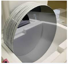
1(GaAs) Gallium Arsenide Wafers
PWAM Develops and manufactures compound semiconductor substrates-gallium arsenide crystal and wafer.We has used advanced crystal growth technology,vertical gradient freeze(VGF) and GaAs wafer processing technology,established a production line from crystal growth, cutting, grinding to polishing processing and built a 100-class clean room for wafer cleaning and packaging. Our GaAs wafer include 2~6 inch ingot/wafers for LED,LD and Microelectronics applications.We are always dedicated to improve the quality of currently substates and develop large size substrates.
(GaAs)Gallium Arsenide Wafers for LED Applications
|
Item |
Specifications |
Remarks |
|
Conduction Type |
SC/n-type |
SC/p-type with Zn dope Available |
|
Growth Method |
VGF |
|
|
Dopant |
Silicon |
Zn available |
|
Wafer Diamter |
2, 3 & 4 inch |
Ingot or as-cut availalbe |
|
Crystal Orientation |
(100)20/60/150 off (110) |
Other misorientation available |
|
OF |
EJ or US |
|
|
Carrier Concentration |
(0.4~2.5)E18/cm3 |
|
|
Resistivity at RT |
(1.5~9)E-3 Ohm.cm |
|
|
Mobility |
1500~3000cm2/V.sec |
|
|
Etch Pit Density |
<5000/cm2 |
|
|
Laser Marking |
upon request |
|
|
Surface Finish |
P/E or P/P |
|
|
Thickness |
220~450um |
|
|
Epitaxy Ready |
Yes |
|
|
Package |
Single wafer container or cassette |
|
(GaAs)Gallium Arsenide Wafers for LD Applications
|
Item |
Specifications |
Remarks |
|
Conduction Type |
SC/n-type |
|
|
Growth Method |
VGF |
|
|
Dopant |
Silicon |
|
|
Wafer Diamter |
2, 3 & 4 inch |
Ingot or as-cut available |
|
Crystal Orientation |
(100)20/60/150 off (110) |
Other misorientation available |
|
OF |
EJ or US |
|
|
Carrier Concentration |
(0.4~2.5)E18/cm3 |
|
|
Resistivity at RT |
(1.5~9)E-3 Ohm.cm |
|
|
Mobility |
1500~3000 cm2/V.sec |
|
|
Etch Pit Density |
<500/cm2 |
|
|
Laser Marking |
upon request |
|
|
Surface Finish |
P/E or P/P |
|
|
Thickness |
220~350um |
|
|
Epitaxy Ready |
Yes |
|
|
Package |
Single wafer container or cassette |
|
(GaAs)Gallium Arsenide Wafers,Semi-insulating for Microelectronics Applications
|
Item |
Specifications |
Remarks |
|
Conduction Type |
Insulating |
|
|
Growth Method |
VGF |
|
|
Dopant |
Undoped |
|
|
Wafer Diamter |
2, 3 & 4 inch |
Ingot available |
|
Crystal Orientation |
(100)+/- 0.50 |
|
|
OF |
EJ, US or notch |
|
|
Carrier Concentration |
n/a |
|
|
Resistivity at RT |
>1E7 Ohm.cm |
|
|
Mobility |
>5000 cm2/V.sec |
|
|
Etch Pit Density |
<8000 /cm2 |
|
|
Laser Marking |
upon request |
|
|
Surface Finish |
P/P |
|
|
Thickness |
350~675um |
|
|
Epitaxy Ready |
Yes |
|
|
Package |
Single wafer container or cassette |
|
6" (GaAs)Gallium Arsenide Wafers,Semi-insulating for Microelectronics Applications
|
Item |
Specifications |
Remarks |
|
Conduction Type |
Semi-insulating |
|
|
Grow Method |
VGF |
|
|
Dopant |
Undoped |
|
|
Type |
N |
|
|
Diamater(mm) |
150±0.25 |
|
|
Orientation |
(100)00±3.00 |
|
|
NOTCH Orientation |
〔010〕±20 |
|
|
NOTCH Deepth(mm) |
(1-1.25)mm 890-950 |
|
|
Carrier Concentration |
N/A |
|
|
Resistivity(ohm.cm) |
>1.0×10⁷ or 0.8-9 x10⁻³ |
|
|
Mobility(cm2/v.s) |
N/A |
|
|
Dislocation |
N/A |
|
|
Thickness(µm) |
675±25 |
|
|
Edge Exclusion for Bow and Warp(mm) |
N/A |
|
|
Bow(µm) |
N/A |
|
|
Warp(µm) |
≤20.0 |
|
|
TTV(µm) |
≤10.0 |
|
|
TIR(µm) |
≤10.0 |
|
|
LFPD(µm) |
N/A |
|
|
Polishing |
P/P Epi-Ready |
|
2" LT-GaAs (Low Temperature-Grown Galium Arsenide) Wafer Specifications
|
Item |
Specifications |
Remarks |
|
Diamater(mm) |
Ф 50.8mm ± 1mm |
|
|
Thickness |
1-2um or 2-3um |
|
|
Marco Defect Density |
≤ 5 cm-2 |
|
|
Resistivity(300K) |
>108 Ohm-cm |
|
|
Carrier |
<0.5ps |
|
|
Dislocation Density |
<1x106cm-2 |
|
|
Useable Surface Area |
≥80% |
|
|
Polishing |
Single side polished |
|
|
Substrate |
GaAs Substrate |
|
* We also can provide poly crystal GaAs bar, 99.9999%(6N).
Remark:
The Chinese government has announced new limits on the exportation of Gallium materials (such as GaAs, GaN, Ga2O3, GaP, InGaAs, and GaSb) and Germanium materials used to make semiconductor chips. Starting from August 1, 2023, exporting these materials is only allowed if we obtains a license from the Chinese Ministry of Commerce. Hope for your understanding and cooperation!
We are manufacturing various types of epi wafer III-V silicon doped n-type semiconductor materials based on Ga, Al, In, As and P grown by MBE or MOCVD. We supply custom structures to meet customer specifications.please contact us for more information.
FZ polished wafers, mainly for the production of silicon rectifier (SR), silicon controlled rectifier (SCR), Giant Transistor (GTR), thyristor (GRO)
We are manufacturing various types of epi wafer III-V silicon doped n-type semiconductor materials based on Ga, Al, In, As and P grown by MBE or MOCVD. We supply custom structures to meet customer specifications.please contact us for more information.
PAM-XIAMEN Offers Photomasks A photo mask is a thin coating of masking material supported by a thicker substrate, and the masking material absorbs light to varying degrees and can be patterned with a custom design. The pattern is used to modulate light and transfer the pattern through the process of photolithography which is the fundamental process1
Xiamen Powerway offers GaSb wafer - gallium antimonide which are grown by LEC(Liquid Encapsulated Czochralski) as epi-ready or mechanical grade with n type, p type or semi-insulating in different orientation(111)or(100)
We provide custom thin film (silicon carbide) SiC epitaxy on 6H or 4H substrates for the development of silicon carbide devices. SiC epi wafer is mainly used for Schottky diodes, metal-oxide semiconductor field-effect transistors, junction field effect transistors, bipolar junction transistors, thyristors, GTO, and insulated gate bipolar.
CZ-Silicon The heavily/lightly-doped CZ mono-crystalline silicon is suitable for producing various integrated circuits (IC), diodes, triodes, green-energy solar panel. The special elements (such as Ga, Ge) can be added to produce the high-efficiency, radiation-resistant and anti-degenerating solar cell materials for special components.
FZ-Silicon The mono-crystalline silicon with the characteristics of low foreign-material content, low defect density and perfect crystal structure is produced with the float-zone process; no foreign material is introduced during the crystal growth. The FZ-Silicon conductivity is usually above 1000 Ω-cm, and the FZ-Silicon is mainly used to produce 1
 Contact Information
 luna@powerwaywafer.compowerwaymaterial@gmail.com
  +86-592-5601 404