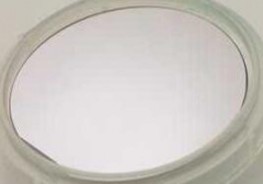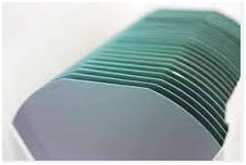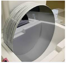
PAM offers semiconductor materials,single crystal (Ge)Germanium Wafer grown by VGF / LEC
MOQ :
1
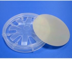
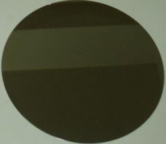
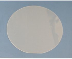
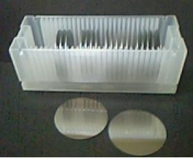
Single crystal (Ge)Germanium Wafer
PAM offers semiconductor materials,Ge(Germanium) Single Crystals and Wafers grown by VGF / LEC
General Properties of Germanium Wafer
|
General Properties Structure |
Cubic, a = 5.6754 Å |
||
|
Density: 5.765 g/cm3 |
|||
|
Melting Point: 937.4 oC |
|||
|
Thermal Conductivity: 640 |
|||
|
Crystal Growth Technology |
Czochralski |
||
|
Doping available |
Undoped |
Sb Doping |
Doping In or Ga |
|
Conductive Type |
/ |
N |
P |
|
Resistivity, ohm.cm |
>35 |
< 0.05 |
0.05 - 0.1 |
|
EPD |
< 5x10³/cm2 |
< 5x10³/cm2 |
< 5x10³/cm2 |
|
< 5x10²/cm2 |
< 5x10²/cm2 |
< 5x10²/cm2 |
|
Grades and Application of Germanium wafer
|
Electronic Grade |
Used for diodes and transistors, |
|
Infrared or opitical Grade |
Used for IR optical window or disks,opitical components |
|
Cell Grade |
Standard Specs of Germanium Crystal and wafer
|
Crystal Orientation |
<111>,<100> and <110> ± 0.5o or custom orientation |
|||
|
Crystal boule as grown |
1" ~ 6" diameter x 200 mm Length |
|||
|
Standard blank as cut |
1"x 0.5mm |
2"x0.6mm |
4"x0.7mm |
5"&6"x0.8mm |
|
Standard Polished wafer(One/two sides polished) |
1"x 0.30 mm |
2"x0.5mm |
4"x0.5mm |
5"&6"x0.6mm |
Special size and orientation are available upon requested Wafers
Specification of Germanium Wafer
|
Item |
Specifications |
Remarks |
|
Growth Method |
VGF |
|
|
Conduction Type |
n-type, p type, undoped |
|
|
Dopant |
Gallium or Antimony |
|
|
Wafer Diamter |
2, 3,4 & 6 |
inch |
|
Crystal Orientation |
(100),(111),(110) |
|
|
Thickness |
200~550 |
um |
|
OF |
EJ or US |
|
|
Carrier Concentration |
request upon customers |
|
|
Resistivity at RT |
(0.001~80) |
Ohm.cm |
|
Etch Pit Density |
<5000 |
/cm2 |
|
Laser Marking |
upon request |
|
|
Surface Finish |
P/E or P/P |
|
|
Epi ready |
Yes |
|
|
Package |
Single wafer container or cassette |
|
|
4 inch Ge wafer Specification |
for Solar Cells |
|
|
Doping |
P |
|
|
Doping substances |
Ge-Ga |
|
|
Diameter |
100±0.25 mm |
|
|
Orientation |
(100) 9° off toward <111>+/-0.5 |
|
|
Off-orientation tilt angle |
N/A |
|
|
Primary Flat Orientation |
N/A |
|
|
Primary Flat Length |
32±1 |
mm |
|
Secondary Flat Orientation |
N/A |
|
|
Secondary Flat Length |
N/A |
mm |
|
cc |
(0.26-2.24)E18 |
/c.c |
|
Resistivity |
(0.74-2.81)E-2 |
ohm.cm |
|
Electron Mobility |
382-865 |
cm2/v.s. |
|
EPD |
<300 |
/cm2 |
|
Laser Mark |
N/A |
|
|
Thickness |
175±10 |
μm |
|
TTV |
<15 |
μm |
|
TIR |
N/A |
μm |
|
BOW |
<10 |
μm |
|
Warp |
<10 |
μm |
|
Front face |
Polished |
|
|
Back face |
Ground |
|
Germanium Wafer Process
In the germanium wafer production process, germanium dioxide from the residue processing is further purified in chlorination and hydrolysis steps.
1)High purity germanium is obtained during zone refining.
2)A germanium crystal is produced via the Czochralski process.
3)The germanium wafer is manufactured via several cutting, grinding, and etching steps.
4)The wafers are cleaned and inspection. During this process, the wafers are single side polished or double side polished according to custom requirement, epi-ready wafer comes.
5)The wafers are packed in single wafer containers, under a nitrogen atmosphere.
Application:
Germanium blank or window are used in night vision and thermographic imaging solutions for commercial security, fire fighting and industrial monitoring equipment. Also, they are used as filters for analytical and measuring equipment, windows for remote temperature measurement, and mirrors for lasers.
Thin Germanium substrates are used in III-V triple-junction solar cells and for power Concentrated PV (CPV) systems.
Remark:
The Chinese government has announced new limits on the exportation of Gallium materials (such as GaAs, GaN, Ga2O3, GaP, InGaAs, and GaSb) and Germanium materials used to make semiconductor chips. Starting from August 1, 2023, exporting these materials is only allowed if we obtains a license from the Chinese Ministry of Commerce. Hope for your understanding and cooperation!
Xiamen Powerway offers GaP wafer - gallium Phosphide which are grown by LEC(Liquid Encapsulated Czochralski) as epi-ready or mechanical grade with n type, p type or semi-insulating in different orientation(111)or(100).
Silicon Epitaxial Wafer(Epi Wafer) is a layer of single crystal silicon deposited onto a single crystal silicon wafer(note: it is available to Grow a layer of poly crystalline Silicon layer on top of a highly doped Singly crystalline Silicon wafer,but it needs buffer layer (such as oxide or poly-Si) in between the bulk Si substrate and the top epit1
Cadmium Zinc Telluride (CdZnTe or CZT) is a new semiconductor, which enables to convert radiation to electron effectively, it is mainly used in infrared thin-film epitaxy substrate,X-ray detectors and Gamma-ray detectors, laser optical modulation, high-performance solar cells and other high-tech fields.
FZ polished wafers, mainly for the production of silicon rectifier (SR), silicon controlled rectifier (SCR), Giant Transistor (GTR), thyristor (GRO)
PAM-XIAMEN has established the manufacturing technology for freestanding (gallium nitride)GaN substrate wafer, which is for UHB-LED and LD. Grown by hydride vapour phase epitaxy (HVPE) technology,Our GaN substrate has low defect density.
Xiamen Powerway offers InP wafer - Indium Phosphide which are grown by LEC(Liquid Encapsulated Czochralski) or VGF(Vertical Gradient Freeze) as epi-ready or mechanical grade with n type, p type or semi-insulating in different orientation(111)or(100).
FZ-Silicon The mono-crystalline silicon with the characteristics of low foreign-material content, low defect density and perfect crystal structure is produced with the float-zone process; no foreign material is introduced during the crystal growth. The FZ-Silicon conductivity is usually above 1000 Ω-cm, and the FZ-Silicon is mainly used to produce 1
PAM-XIAMEN Offers Dummy Wafer / Test Wafer / Monitor Wafer
 Contact Information
 luna@powerwaywafer.compowerwaymaterial@gmail.com
  +86-592-5601 404