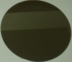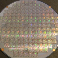
Xiamen Powerway offers InSb wafer - Indium antimonide which are grown by LEC(Liquid Encapsulated Czochralski) as epi-ready or mechanical grade with n type, p type or semi-insulating in different orientation(111)or(100).
Xiamen Powerway offers InSb wafer - Indium antimonide which are grown by LEC(Liquid Encapsulated Czochralski) as epi-ready or mechanical grade with n type, p type or semi-insulating in different orientation(111)or(100).
Indium antimonide (InSb) is a crystalline compound made from the elements indium (In) and antimony (Sb). It is a narrow-gap semiconductor material from the III-V group used in infrared detectors, including thermal imaging cameras,FLIR systems, infrared homing missile guidance systems, and in infrared astronomy. The indium antimonide detectors are sensitive between 1–5 µm wavelengths. Indium antimonide was a very common detector in the old, single-detector mechanically scanned thermal imaging systems. Another application is as a terahertz radiation source as it is a strong photo-Dember emitter.
| Wafer Specification | |
| Item | Specifications |
| Wafer Diameter |
2"50.5±0.5mm 3"76.2±0.4mm 4"1000.0±0.5mm |
| Crystal Orientation |
2"(111)AorB±0.1° 3"(111)AorB±0.1° 4"(111)AorB±0.1° |
| Thickness |
2"625±25um 3" 800or900±25um 4"1000±25um |
| Primary flat length |
2"16±2mm 3"22±2mm 4"32.5±2.5mm |
| Secondary flat length |
2"8±1mm 3"11±1mm 4"18±1mm |
| Surface Finish | P/E, P/P |
| Package | Epi-Ready,Single wafer container or CF cassette |
| Electrical and Doping Specification | |||||
| Conduction Type | n-type | n-type | n-type | n-type | p-type |
| Dopant | Undoped | Tellurium | Low tellurium | High tellurium | Genmanium |
| E.D.P cm-2 | 2"3"4"≤50 | 2"≤100 | |||
| Mobility cm² V-1s-1 | ≥4*105 | ≥2.5*104 | ≥2.5*105 | Not Specified | 8000-4000 |
| Carrier Concentration cm-3 | 5*1013-3*1014 | (1-7)*1017 | 4*1014-2*1015 | ≥1*1018 | 5*1014-3*1015 |
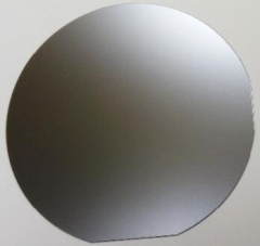
Xiamen Powerway offers InP wafer - Indium Phosphide which are grown by LEC(Liquid Encapsulated Czochralski) or VGF(Vertical Gradient Freeze) as epi-ready or mechanical grade with n type, p type or semi-insulating in different orientation(111)or(100).
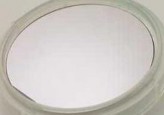
Xiamen Powerway offers InAs wafer - Indium arsenide which are grown by LEC(Liquid Encapsulated Czochralski) as epi-ready or mechanical grade with n type, p type or semi-insulating in different orientation(111)or(100).
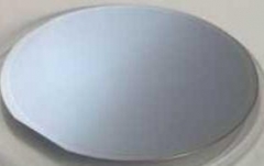
Xiamen Powerway offers GaP wafer - gallium Phosphide which are grown by LEC(Liquid Encapsulated Czochralski) as epi-ready or mechanical grade with n type, p type or semi-insulating in different orientation(111)or(100).
Xiamen Powerway offers GaSb wafer - gallium antimonide which are grown by LEC(Liquid Encapsulated Czochralski) as epi-ready or mechanical grade with n type, p type or semi-insulating in different orientation(111)or(100)
We are manufacturing various types of epi wafer III-V silicon doped n-type semiconductor materials based on Ga, Al, In, As and P grown by MBE or MOCVD. We supply custom structures to meet customer specifications.please contact us for more information.
PAM-XIAMEN's Template Products consist of crystalline layers of gallium nitride (GaN), aluminum nitride (AlN),aluminum gallium nitride (AlGaN)and indium gallium nitride (InGaN), which are deposited on sapphire substrates, silicon carbide or silicon.PAM-XIAMEN's Template Products enable 20-50% shorter epitaxy cycle times and higher quality epitaxial1
PAM-XIAMEN Offers photoresist plate with photoresist We can offer Nanolithography (photolithography):Surface preparation, Photoresist apply, Soft bake, Alignment, Exposure, Development,Hard bake, Develop inspect, Etch, Photoresist removal(strip), Final inspection.
Cadmium Zinc Telluride (CdZnTe or CZT) is a new semiconductor, which enables to convert radiation to electron effectively, it is mainly used in infrared thin-film epitaxy substrate,X-ray detectors and Gamma-ray detectors, laser optical modulation, high-performance solar cells and other high-tech fields.
 Contact Information
 luna@powerwaywafer.compowerwaymaterial@gmail.com
  +86-592-5601 404