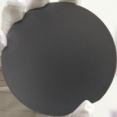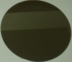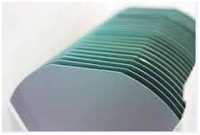
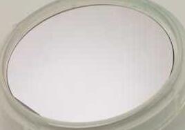
Xiamen Powerway offers GaSb wafer - gallium antimonide which are grown by LEC(Liquid Encapsulated Czochralski) as epi-ready or mechanical grade with n type, p type or semi-insulating in different orientation(111)or(100)
MOQ :
1Xiamen Powerway offers GaSb wafer - gallium antimonide which are grown by LEC(Liquid Encapsulated Czochralski) as epi-ready or mechanical grade with n type, p type or semi-insulating in different orientation(111)or(100).
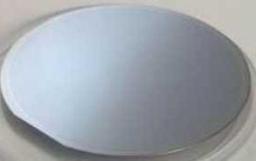
Gallium antimonide (GaSb) is a semiconducting compound of gallium and antimony of the III-V family.It has a lattice constant of about 0.61 nm. GaSb can be used for Infrared detectors,infrared LEDs and lasers and transistors, and thermophotovoltaic systems.
Wafer Specification
Item
Specifications
Wafer Diameter
2"50.5±0.5mm
3"76.2±0.4mm
4"1000.0±0.5mm
Crystal Orientation
(100)±0.1°
Thickness
2"500±25um
3" 625±25um
4"1000±25um
Primary flat length
2"16±2mm
3"22±2mm
4"32.5±2.5mm
Secondary flat length
2"8±1mm
3"11±1mm
4"18±1mm
Surface Finish
P/E, P/P
Package
Epi-Ready,Single wafer container or CF cassette
| Electrical and Doping Specification | |||||
| Conduction Type | p-type | p-type | n-type | n-type | n-type |
| Dopant | Undoped | Zinc | Tellurium | Low tellurium | High tellurium |
| E.D.P cm-2 |
2"≤2000 3"≤5000 |
2"≤2000 3"≤5000 |
2",3"≤1000 4"≤2000 |
2"≤1000 3",4"≤2000 |
2,"3",4"≤500 |
| Mobility cm² V-1s-1 | ≥500 | 450-200 | 3500-2000 | 3500-2000 | 3500-2000 |
| Carrier Concentration cm-3 | ≤2*1017 | ≥1*1018 | (91-900)*1017 | ≤2*1017 |
≥5*1017 |
Remark:
The Chinese government has announced new limits on the exportation of Gallium materials (such as GaAs, GaN, Ga2O3, GaP, InGaAs, and GaSb) and Germanium materials used to make semiconductor chips. Starting from August 1, 2023, exporting these materials is only allowed if we obtains a license from the Chinese Ministry of Commerce. Hope for your understanding and cooperation!
Xiamen Powerway offers InSb wafer - Indium antimonide which are grown by LEC(Liquid Encapsulated Czochralski) as epi-ready or mechanical grade with n type, p type or semi-insulating in different orientation(111)or(100).
Xiamen Powerway offers InP wafer - Indium Phosphide which are grown by LEC(Liquid Encapsulated Czochralski) or VGF(Vertical Gradient Freeze) as epi-ready or mechanical grade with n type, p type or semi-insulating in different orientation(111)or(100).
Xiamen Powerway offers InAs wafer - Indium arsenide which are grown by LEC(Liquid Encapsulated Czochralski) as epi-ready or mechanical grade with n type, p type or semi-insulating in different orientation(111)or(100).
Xiamen Powerway offers GaP wafer - gallium Phosphide which are grown by LEC(Liquid Encapsulated Czochralski) as epi-ready or mechanical grade with n type, p type or semi-insulating in different orientation(111)or(100).
PWAM Develops and manufactures compound semiconductor substrates-gallium arsenide crystal and wafer.We has used advanced crystal growth technology,vertical gradient freeze(VGF) and GaAs wafer processing technology,established a production line from crystal growth, cutting, grinding to polishing processing and built a 100-class clean room for 1
Silicon Epitaxial Wafer(Epi Wafer) is a layer of single crystal silicon deposited onto a single crystal silicon wafer(note: it is available to Grow a layer of poly crystalline Silicon layer on top of a highly doped Singly crystalline Silicon wafer,but it needs buffer layer (such as oxide or poly-Si) in between the bulk Si substrate and the top epit1
Cadmium Zinc Telluride (CdZnTe or CZT) is a new semiconductor, which enables to convert radiation to electron effectively, it is mainly used in infrared thin-film epitaxy substrate,X-ray detectors and Gamma-ray detectors, laser optical modulation, high-performance solar cells and other high-tech fields.
PAM-XIAMEN has established the manufacturing technology for freestanding (gallium nitride)GaN substrate wafer, which is for UHB-LED and LD. Grown by hydride vapour phase epitaxy (HVPE) technology,Our GaN substrate has low defect density.
 Contact Information
 luna@powerwaywafer.compowerwaymaterial@gmail.com
  +86-592-5601 404