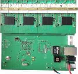
PAM-XIAMEN provides CZT based detectors by solid-state detector technology for x-ray or gamma-ray,which has better energy resolution compared with scintillation crystal based detector, including CZT Planar Detector,CZT Pixilated Detector,CZT Co-Planar Gri
CZT Detector
1.1CZT Planar Detector
Specifications
|
HV |
+200 V~ +500 V |
||
|
Energy range |
20 KeV ~ 200 KeV |
||
|
Operating temperature range |
-20℃ ~ 40℃ |
||
|
Size(mm 3 ) |
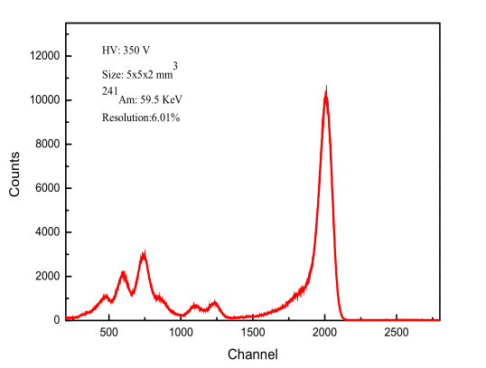
5×5×2 |
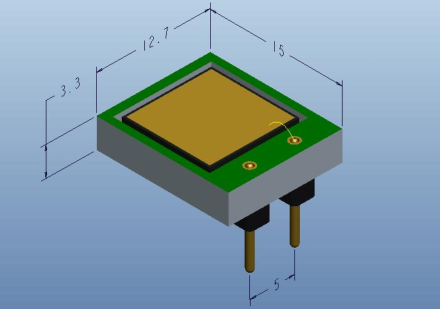
10×10×2 |
|
|
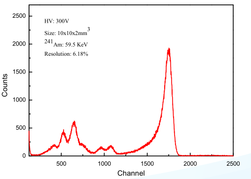
Energy resolution @59.5 KeV |
Counter grade |
>15% |
>15% |
|
Discriminator grade |
7% ~ 15% |
8% ~ 15% |
|
|
Spectrometer grade |
<7% |
<8% |
|
|
Note |
|
Other sizes can also be available |
|
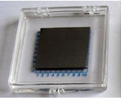
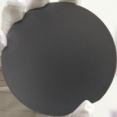
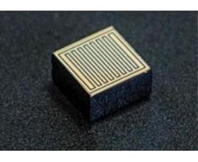
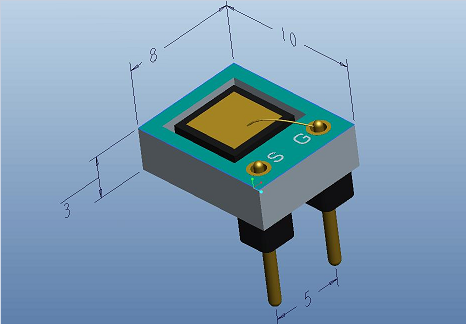
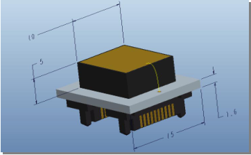
Standard 5×5×2mm 3 CZT assembly
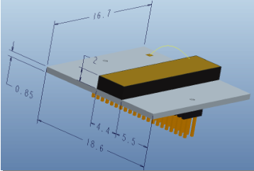
Standard 10×10×2mm 3 CZT assembly
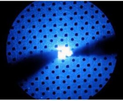
1.2CZT Pixilated Detector
Specifications
|
Application |
SPECT、γ Camera |
X-ray imaging |
|
Operating temperature range |
-20℃ ~ 40℃ |
|
|
Typical energy resolution |
<6.5%@59.5 KeV |
—— |
|
Count rate |
—— |
>2M cps/pixel |
|
Typical matrix |
Area array detector: 8×8 |
Area array detector: 8×8 |
|
Linear array detector: 1×16 |
Linear array detector: 1×16 |
|
|
The maximum dimensions of crystal |
40×40×5 mm 3 |
|
|
Note |
Other electrode pattern can also be available |
|
Standard 8×8 pixel CZT detector assembly
Standard 8×8 pixel CZT detector assembly
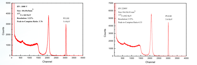
1.3CZT Co-Planar Grid Detectors
Specifications
HV: +1000 V ~ +3000V
Energy range: 50 KeV ~ 3 MeV
Operating temperature range:-20℃ ~ 40℃
Typical energy resolution:<4%@662 KeV
Peak-to-Compton ratio: 3 ~ 5
Standard size(mm 3 ): 10×10×5, 10×10×10
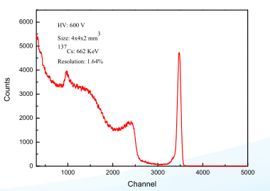
1.4CZT Hemispherical Detector
HV: +200 V ~ +1000 V Operating temperature range:-20℃ ~ 40℃
Energy range: 50 KeV ~ 3 MeV Typical energy resolution:<3%@662 KeV
Standard size(mm 3 ) :4×4×2, 5×5×2.5, 10×10×5
Cadmium Zinc Telluride (CdZnTe or CZT) is a new semiconductor, which enables to convert radiation to electron effectively, it is mainly used in infrared thin-film epitaxy substrate,X-ray detectors and Gamma-ray detectors, laser optical modulation, high-performance solar cells and other high-tech fields.
Xiamen Powerway offers InSb wafer - Indium antimonide which are grown by LEC(Liquid Encapsulated Czochralski) as epi-ready or mechanical grade with n type, p type or semi-insulating in different orientation(111)or(100).
Due to SiC physical and electronic properties,Silicon Carbide based device are well suitable for short wavelength optoelectronic, high temperature, radiation resistant, and high-power/high-frequency electronic devices,compared with Si and GaAs based device.
Cadmium Zinc Telluride (CdZnTe or CZT) is a new semiconductor, which enables to convert radiation to electron effectively, it is mainly used in infrared thin-film epitaxy substrate,X-ray detectors and Gamma-ray detectors, laser optical modulation, high-performance solar cells and other high-tech fields.
CZ-Silicon The heavily/lightly-doped CZ mono-crystalline silicon is suitable for producing various integrated circuits (IC), diodes, triodes, green-energy solar panel. The special elements (such as Ga, Ge) can be added to produce the high-efficiency, radiation-resistant and anti-degenerating solar cell materials for special components.
We are manufacturing various types of epi wafer III-V silicon doped n-type semiconductor materials based on Ga, Al, In, As and P grown by MBE or MOCVD. We supply custom structures to meet customer specifications.please contact us for more information.
Gallium Nitride (GaN) HEMTs (High Electron Mobility Transistors) are the next generation of RF power transistor technology.Thanks to GaN technology,PAM-XIAMEN now offer AlGaN/GaN HEMT Epi Wafer on sapphire or Silicon,and AlGaN/GaN on sapphire template.
PAM-XIAMEN's GaN(gallium nitride)-based LED epitaxial wafer is for ultra high brightness blue and green light emitting diodes (LED) and laser diodes (LD) application.
 Contact Information
 luna@powerwaywafer.compowerwaymaterial@gmail.com
  +86-592-5601 404