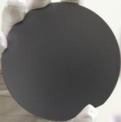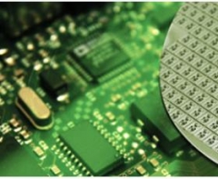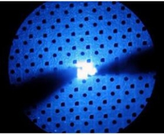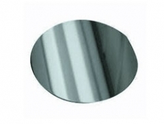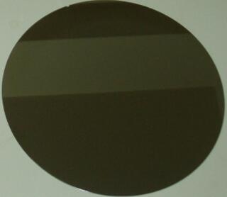
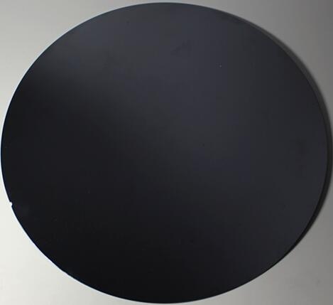
Xiamen Powerway offers InP wafer - Indium Phosphide which are grown by LEC(Liquid Encapsulated Czochralski) or VGF(Vertical Gradient Freeze) as epi-ready or mechanical grade with n type, p type or semi-insulating in different orientation(111)or(100).
Xiamen Powerway offers InP wafer - Indium Phosphide which are grown by LEC(Liquid Encapsulated Czochralski) or VGF(Vertical Gradient Freeze) as epi-ready or mechanical grade with n type, p type or semi-insulating in different orientation(111)or(100).
Indium phosphide (InP) is a binary semiconductor composed of indium and phosphorus. It has a face-centered cubic ("zinc blende") crystal structure, identical to that of GaAs and most of the III-V semiconductors.Indium phosphide can be prepared from the reaction of white phosphorus and indium iodide[clarification needed] at 400 °C.,[5] also by direct combination of the purified elements at high temperature and pressure, or by thermal decomposition of a mixture of a trialkyl indium compound and phosphide. InP is used in high-power and high-frequency electronics[citation needed] because of its superior electron velocity with respect to the more common semiconductors silicon and gallium arsenide.
| Wafer Specification | |
| Item | Specifications |
| Wafer Diameter | 50.5±0.4mm |
| Crystal Orientation | (100)±0.1° |
| Thickness | 350±25um / 500±25um |
| Primary flat length | 16±2mm |
| Secondary flat length | 8±1mm |
| Surface Finish | P/E, P/P |
| Package | Epi-Ready,Single wafer container or CF cassette |
| Electrical and Doping Specification | ||||||
| Conduction Type | n-type | n-type | n-type | n-type | p-type | p-type |
| Dopant | Undoped | Iron | Tin | Sulphur | Zinc | Low Zinc |
| E.D.P cm-2 | ≤5000 | ≤5000 | ≤50000 | ≤1000 | ≤1000 | ≤5000 |
| Mobility cm² V-1s-1 | ≥4200 | ≥1000 | 2500-750 | 2000-1000 | Not Specified | Not Specified |
| Carrier Concentration cm-3 | ≤1016 | Semi-Insulating | (7-40)*1017 | (1-10)*1018 | (1-6)*1018 | (1-6)*101 |
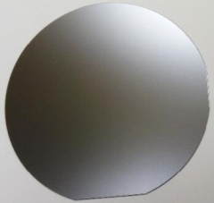
Xiamen Powerway offers InSb wafer - Indium antimonide which are grown by LEC(Liquid Encapsulated Czochralski) as epi-ready or mechanical grade with n type, p type or semi-insulating in different orientation(111)or(100).
Xiamen Powerway offers InAs wafer - Indium arsenide which are grown by LEC(Liquid Encapsulated Czochralski) as epi-ready or mechanical grade with n type, p type or semi-insulating in different orientation(111)or(100).
Xiamen Powerway offers GaP wafer - gallium Phosphide which are grown by LEC(Liquid Encapsulated Czochralski) as epi-ready or mechanical grade with n type, p type or semi-insulating in different orientation(111)or(100).
Xiamen Powerway offers GaSb wafer - gallium antimonide which are grown by LEC(Liquid Encapsulated Czochralski) as epi-ready or mechanical grade with n type, p type or semi-insulating in different orientation(111)or(100)
Due to SiC physical and electronic properties,Silicon Carbide based device are well suitable for short wavelength optoelectronic, high temperature, radiation resistant, and high-power/high-frequency electronic devices,compared with Si and GaAs based device.
PAM-XIAMEN's GaN(gallium nitride)-based LED epitaxial wafer is for ultra high brightness blue and green light emitting diodes (LED) and laser diodes (LD) application.
CZ-Silicon The heavily/lightly-doped CZ mono-crystalline silicon is suitable for producing various integrated circuits (IC), diodes, triodes, green-energy solar panel. The special elements (such as Ga, Ge) can be added to produce the high-efficiency, radiation-resistant and anti-degenerating solar cell materials for special components.
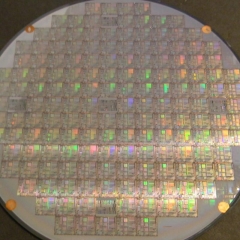
PAM-XIAMEN Offers photoresist plate with photoresist We can offer Nanolithography (photolithography):Surface preparation, Photoresist apply, Soft bake, Alignment, Exposure, Development,Hard bake, Develop inspect, Etch, Photoresist removal(strip), Final inspection.
 Contact Information
 luna@powerwaywafer.compowerwaymaterial@gmail.com
  +86-592-5601 404