AlGaInP is used in manufacture of light-emitting diodes of high-brightness red, orange, green, and yellow color, to form the heterostructure emitting light. It is also used to make diode lasers.
AlGaInP layer is often grown by heteroepitaxy on gallium arsenide or gallium phosphide in order to form a quantum well structure.

Specs of AlGaInP wafers on chips
AlGaInP LED Wafer for chip
Item No.:PAM-CAYG1101
Dimensions:
Growth Technique – MOCVD
Substrate Material: Gallium arsenide
Substrate Conduction: n type
Diameter:2"
●Chip Dimensions:
1)Chip size:front size:8mil(±1mil)×8mil(±1mil)
back side:9mil(±1mil)×9mil(±1mil)
2)Chip thickness:7mil(±1mil)
3)Pad size:4mil(±0.5mil)
4)Structure:see 1-1
●Photoelectric Properties
|
Parameter |
Condition |
Min. |
Typ. |
Max. |
Unit |
|
Forward Voltage(Vf1) |
If=10μA |
1.35 |
﹎ |
﹎ |
V |
|
Forward Voltage(Vf2) |
If=20mA |
﹎ |
﹎ |
2.2 |
V |
|
Reverse Voltage(Lr) |
Vr=10V |
﹎ |
﹎ |
2 |
μA |
|
Dominant wavelength(λd) |
If=20mA |
565 |
﹎ |
575 |
nm |
|
FWHM(Δλ) |
If=20mA |
﹎ |
10 |
﹎ |
nm |
●Luminous Intensity:
|
Code |
LC |
LD |
LE |
LF |
LG |
LH |
LI |
|
IV(mcd) |
20-30 |
25-35 |
30-35 |
35-50 |
40-60 |
50-70 |
60-80 |
Band gap of strained AlGaInP on GaAs substrate
In this tutorial we want to study the band gaps of strained AlxGayIn1-x-yP on a GaAs substrate.
The material parameters are taken from
Band parameters for III-V compound semiconductors and their alloys
I. Vurgaftman, J.R. Meyer, L.R. Ram-Mohan
J. Appl. Phys. 89 (11), 5815 (2001)
To understand the effect of strain on the band gap on the individual components of this quaternary, we first examine the effects on
|
1)AlP |
strained tensilely |
with respect to GaAs |
|
2)GaP |
strained tensilely |
with respect to GaAs |
|
3)InP |
strained compressively |
with respect to GaAs |
|
4)AlxGa1-xP |
strained tensilely |
with respect to GaAs |
|
5)GaxIn1-xP |
strained |
with respect to GaAs |
|
6)AlxIn1-xP |
strained |
with respect to GaAs |
|
7)Al0.4Ga0.6P |
strained tensilely |
with respect to GaAs |
|
8)Ga0.4In0.6P |
strained compressively |
with respect to GaAs |
|
9)Al0.4In0.6P |
strained compressively |
with respect to GaAs |
Each material layer has a length of 10 nm in the simulation.
The material layers 4), 5) and 6) vary its alloy contents linearly:
|
4)AlxGa1-xP from 10 nm to 20 nm from x=0.0 to x=1.0 |
|
5)GaxIn1-xP from 30 nm to 40 nm from x=0.0 to x=1.0 |
|
6)AlxIn1-xP from 50 nm to 60 nm from x=1.0 to x=0.0 |
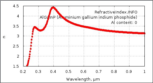
Refractive index of AlGaInP
Source: PAM-XIAMEN
For more information, please visit our website: www.semiconductorwafers.net,
send us email at luna@powerwaywafer.com or powerwaymaterial@gmail.com.
 Contact Information
 luna@powerwaywafer.compowerwaymaterial@gmail.com
  +86-592-5601 404


