PAM XIAMEN Offers Epitaxial growth of AlGaN/GaN based HEMT on Si wafers
Recently, PAM XIAMEN, a leading supplier of GaN epitaxial wafers, announced that it has successfully developed "6-inch silicon-on-silicon (GaN-on-Si) epitaxial wafers" and its 6 inch size is on mass production.
PAM XIAMEN is effective in third-generation semiconductors
In order to lay out and grasp the development opportunities of the wide bandgap compound semiconductor materials (i.e. the third generation semiconductor materials) industry, PAM XIAMEN has been invested in research and development continuously, the data show that PAM XIAMEN is mainly engaged in the design, development and production of semiconductor materials, especially gallium nitride (GaN) epitaxial materials, focusing on the application of related materials in avionics, 5G communication, Internet of Things and other fields, Improving and enriching the company's industrial chain.
Since its inception, PAM XIAMEN has overcome the technical difficulties of lattice mismatch, large-scale epitaxial stress control, and high-voltage GaN epitaxial growth between GaN and Si materials, and successfully developed a 8-inch silicon-based Gallium Nitride epi wafers that has reached the world's leading leve, and the 6 inch size wafer is on mass production, our general structure is now as follows:
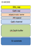
Chart 1: D-MODE
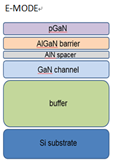
Chart 2: E-MODE
It is understood that this type of epitaxial wafer achieves high voltage resistance of 650V/700V while maintaining high crystal quality, high uniformity and high reliability of epitaxial materials. It can fully meet the application requirements of high voltage power electronic devices in the industry.
According to PAM XIAMEN, In the case of adopting the international industry's stringent criteria, Epitaxial wafers developed by PAM XIAMEN have performance advantages in terms of materials, mechanics, electricity, withstand voltage, high temperature resistance, and longevity. In the fields of 5G communication, cloud computing, fast charging source, wireless charging, etc., it can ensure the safe and reliable application of related materials and technologies.
About Xiamen Powerway Advanced Material Co., Ltd
Found in 1990, Xiamen Powerway Advanced Material Co., Ltd (PAM-XIAMEN), a leading manufacturer of Wide bandgap(WBG) semiconductor material in China, its business involves GaN material covering GaN substrate, AlGaN/GaN HEMT epi wafers on Silicon carbide/Silicon/Sapphire substrate.(Click to read GaN HEMT Epitaxial Wafer details.)
Q&A
Q: Can you please inform us what is the difference between d mode and e mode wafers?
A: There are the difference in two main points:1/Barrier structure,the typical value of D-mode is AlGaN~21nm, Al%~25%,
while it is AlGaN~18nm and Al%~20% in E-mode2/E-HEMT,there are ~100nm P-GaN for deplete 2DEG
Q: We are planning to work on both types of the devices. So I will discuss this with my colleagues.
Can you please inform me about the differences of those wafers.
I mean what is the epi difference between the E mode and D mode wafers.
This will help me more. By the way do you have data for 600V operation with those wafers
A: If it is 600V operation, D-mode is suggested.
Q: I measured the surface of one of the sample with our AFM,the surface is in spec with your measurement.The problem is underneath the surface since it is possible to notice a not smooth surface.
A: I probably understand what you meant, you worried that under optical conditions,the surface roughness will affect the two-dimensional electron gas mobility?
In general, our sample mobility is >1500 cm2/Vs. We will do a batch of Hall test next week,including the same batch of samples shipped this time, and we will send the data back to you.If the hall data does not meet the requirements, we will cooperate with you to do the next work.
In addition, I would like to briefly introduce that there are two uses for similar samples of customer demand: 1. Power devices 2. RF devices. RF devices do not require high material withstand voltage,while power devices require high levels. For Power devices we have adopted C-doping technology,so the crystal quality is not as good as RF devices, and the appearance is relatively rough. Both of
these samples can be provided. Next time, you please consult the conductivity of the substrate, what materials are used for the pressure-resistant layer, and whether the square-resistance mobility has specific requirements.
KeyWords: algan hemt, algan band gap, algan gan hemt, algan gan band diagram,fet transistor,gan power transistor, gan rf, gan on si hemt, gan device,algan/gan hemt, hemt amplifier, gan lattice, gan hemts, gan market
For more information, please visit our website: www.semiconductorwafers.net,send us email at sales@powerwaywafer.com or powerwaymaterial@gmail.com.
 Contact Information
 luna@powerwaywafer.compowerwaymaterial@gmail.com
  +86-592-5601 404


